Millions of years of evolution has resulted in plants being the most
efficient harvesters of solar energy on the planet. Much research is
underway into ways to artificially mimic photosynthesis in devices like artificial leaves,
but researchers at the University of Georgia (UGA) are working on a
different approach that gives new meaning to the term “power plant.”
Their technology harvests energy generated through photosynthesis before
the plants can make use of it, allowing the energy to instead be used
to run low-powered electrical devices.
Photosynthesis turns light energy into chemical energy by splitting
water atoms into hydrogen and oxygen. This process produces electrons
that help create sugars that the plant uses to fuel growth and
reproduction. A team led by Ramaraja Ramasamy, assistant professor in
the UGA College of Engineering, is developing technology that would
interrupt the photosynthesis process and capture the electrons before
the plant puts them to use creating sugars.
The technology involves interrupting the pathways along which the
electrons flow by manipulating the proteins contained in thylakoids.
Thylakoids are membrane-bound compartments at the site of the light
reactions of photosynthesis that are responsible for capturing and
storing energy from sunlight.
The modified thylakoids are immobilized on a specially designed
backing of carbon nanotubes that acts as an electrical conductor to
capture the electrons and send them along a wire. The researchers say
that small-scale experiments of this system have yielded a maximum
current density that is two orders of magnitude larger than previously
reported for similar systems.
While you won’t be running your HDTV off the nearest tree anytime
soon, Ramasamy says the technology has the potential to find its way
into less power-intensive applications in the not too distant future.
"In the near term, this technology might best be used for remote
sensors or other portable electronic equipment that requires less power
to run," he said. "If we are able to leverage technologies like genetic
engineering to enhance stability of the plant photosynthetic
machineries, I'm very hopeful that this technology will be competitive
to traditional solar panels in the future."
Ramasamy and his team are already working to improve the stability
and output of the technology to get it to a stage suitable for
commercialization.
"We have discovered something very promising here, and it is
certainly worth exploring further," he said. "The electrical output we
see now is modest, but only about 30 years ago, hydrogen fuel cells were
in their infancy, and now they can power cars, buses and even
buildings."
But
Contractor, a mechanical engineer with a background in 3D
printing, envisions a much more mundane—and ultimately more
important—use for the technology. He sees a day when every kitchen has a
3D printer, and the earth’s 12 billion people feed themselves
customized, nutritionally-appropriate meals synthesized one layer at a
time, from cartridges of powder and oils they buy at the corner grocery
store. Contractor’s vision would mean the end of food waste, because the
powder his system will use is shelf-stable for up to 30 years, so that
each cartridge, whether it contains sugars, complex carbohydrates,
protein or some other basic building block, would be fully exhausted
before being returned to the store.
Ubiquitous food synthesizers
would also create new ways of producing the basic calories on which we
all rely. Since a powder is a powder, the inputs could be anything that
contain the right organic molecules. We already know that eating meat is
environmentally unsustainable, so why not get all our protein from insects?
If eating something spat out by the same kind of 3D printers that are currently being used to make everything from jet engine parts to fine art
doesn’t sound too appetizing, that’s only because you can currently
afford the good stuff, says Contractor. That might not be the case once
the world’s population reaches its peak size, probably sometime near the end of this century.
“I
think, and many economists think, that current food systems can’t
supply 12 billion people sufficiently,” says Contractor. “So we
eventually have to change our perception of what we see as food.”
There will be pizza on Mars
The ultimate in molecular gastronomy. (Schematic of SMRC’s 3D printer for food.)SMRC
If
Contractor’s utopian-dystopian vision of the future of food ever comes
to pass, it will be an argument for why space research isn’t a complete
waste of money. His initial grant from NASA, under its Small Business
Innovation Research program, is for a system that can print food for
astronauts on very long space missions. For example, all the way to
Mars.
“Long distance space travel requires 15-plus years of shelf
life,” says Contractor. “The way we are working on it is, all the carbs,
proteins and macro and micro nutrients are in powder form. We take
moisture out, and in that form it will last maybe 30 years.”
Pizza
is an obvious candidate for 3D printing because it can be printed in
distinct layers, so it only requires the print head to extrude one
substance at a time. Contractor’s “pizza printer” is still at the
conceptual stage, and he will begin building it within two weeks. It
works by first “printing” a layer of dough, which is baked at the same
time it’s printed, by a heated plate at the bottom of the printer. Then
it lays down a tomato base, “which is also stored in a powdered form,
and then mixed with water and oil,” says Contractor.
Finally, the
pizza is topped with the delicious-sounding “protein layer,” which could
come from any source, including animals, milk or plants.
The prototype for Contractor’s pizza printer (captured in a video,
above) which helped him earn a grant from NASA, was a simple chocolate
printer. It’s not much to look at, nor is it the first of its kind, but at least it’s a proof of concept.
Replacing cookbooks with open-source recipes
SMRC’s prototype 3D food printer will be based on open-source hardware from the RepRap project.RepRap
Remember
grandma’s treasure box of recipes written in pencil on yellowing note
cards? In the future, we’ll all be able to trade recipes directly, as
software. Each recipe will be a set of instructions that tells the
printer which cartridge of powder to mix with which liquids, and at what
rate and how it should be sprayed, one layer at time.
This will
be possible because Contractor plans to keep the software portion of his
3D printer entirely open-source, so that anyone can look at its code,
take it apart, understand it, and tweak recipes to fit. It would of
course be possible for people to trade recipes even if this printer were
proprietary—imagine something like an app store, but for recipes—but
Contractor believes that by keeping his software open source, it will be
even more likely that people will find creative uses for his
hardware. His prototype 3D food printer also happens to be based on a
piece of open-source hardware, the second-generation RepRap 3D printer.
“One
of the major advantage of a 3D printer is that it provides personalized
nutrition,” says Contractor. “If you’re male, female, someone is
sick—they all have different dietary needs. If you can program your
needs into a 3D printer, it can print exactly the nutrients that person
requires.”
Replacing farms with sources of environmentally-appropriate calories
2032: Delicious Uncle Sam’s Meal Cubes are laser-sintered from granulated mealworms; part of this healthy breakfast.TNO Research
Contractor
is agnostic about the source of the food-based powders his system uses.
One vision of how 3D printing could make it possible to turn just about
any food-like starting material into an edible meal was outlined by TNO
Research, the think tank of TNO, a Dutch holding company that owns a
number of technology firms.
In TNO’s vision of a future of 3D printed meals, “alternative ingredients” for food include:
algae
duckweed
grass
lupine seeds
beet leafs
insects
From astronauts to emerging markets
While
Contractor and his team are initially focusing on applications for
long-distance space travel, his eventual goal is to turn his system for
3D printing food into a design that can be licensed to someone who wants
to turn it into a business. His company has been “quite successful in
doing that in the past,” and has created both a gadget that uses microwaves to evaluate the structural integrity of aircraft panels and a kind of metal screw that coats itself with protective sealant once it’s drilled into a sheet of metal.
Since
Contractor’s 3D food printer doesn’t even exist in prototype form, it’s
too early to address questions of cost or the healthiness (or not) of
the food it produces. But let’s hope the algae and cricket pizza turns
out to be tastier than it sounds.
Equinix’s data center in
Secaucus is highly coveted space for financial traders, given its
proximity to the servers that move trades for Wall Street.
The trophy high-rises on Madison, Park and Fifth Avenues in Manhattan
have long commanded the top prices in the country for commercial real
estate, with yearly leases approaching $150 a square foot. So it is
quite a Gotham-size comedown that businesses are now paying rents four
times that in low, bland buildings across the Hudson River in New
Jersey.
Why pay $600 or more a square foot at unglamorous addresses like
Weehawken, Secaucus and Mahwah? The answer is still location, location,
location — but of a very different sort.
Companies are paying top dollar to lease space there in buildings called
data centers, the anonymous warrens where more and more of the world’s
commerce is transacted, all of which has added up to a tremendous boon
for the business of data centers themselves.
The centers provide huge banks of remote computer storage, and the
enormous amounts of electrical power and ultrafast fiber optic links
that they demand.
Prices are particularly steep in northern New Jersey because it is also
where data centers house the digital guts of the New York Stock Exchange
and other markets. Bankers and high-frequency traders are vying to have
their computers, or servers, as close as possible to those markets.
Shorter distances make for quicker trades, and microseconds can mean
millions of dollars made or lost.
When the centers opened in the 1990s as quaintly termed “Internet
hotels,” the tenants paid for space to plug in their servers with a
proviso that electricity would be available. As computing power has
soared, so has the need for power, turning that relationship on its
head: electrical capacity is often the central element of lease
agreements, and space is secondary.
A result, an examination shows, is that the industry has evolved from a
purveyor of space to an energy broker — making tremendous profits by
reselling access to electrical power, and in some cases raising
questions of whether the industry has become a kind of wildcat power
utility.
Even though a single data center can deliver enough electricity to power
a medium-size town, regulators have granted the industry some of the
financial benefits accorded the real estate business and imposed none of
the restrictions placed on the profits of power companies.
Some of the biggest data center companies have won or are seeking
Internal Revenue Service approval to organize themselves as real estate
investment trusts, allowing them to eliminate most corporate taxes. At
the same time, the companies have not drawn the scrutiny of utility
regulators, who normally set prices for delivery of the power to
residences and businesses.
While companies have widely different lease structures, with prices
ranging from under $200 to more than $1,000 a square foot, the
industry’s performance on Wall Street has been remarkable. Digital Realty Trust,
the first major data center company to organize as a real estate trust,
has delivered a return of more than 700 percent since its initial
public offering in 2004, according to an analysis by Green Street
Advisors.
The stock price of another leading company, Equinix,
which owns one of the prime northern New Jersey complexes and is
seeking to become a real estate trust, more than doubled last year to
over $200.
“Their business has grown incredibly rapidly,” said John Stewart, a
senior analyst at Green Street. “They arrived at the scene right as
demand for data storage and growth of the Internet were exploding.”
Push for Leasing
While many businesses own their own data centers — from stacks of
servers jammed into a back office to major stand-alone facilities — the
growing sophistication, cost and power needs of the systems are driving
companies into leased spaces at a breakneck pace.
The New York metro market now has the most rentable square footage in
the nation, at 3.2 million square feet, according to a recent report by
451 Research, an industry consulting firm. It is followed by the
Washington and Northern Virginia area, and then by San Francisco and
Silicon Valley.
A major orthopedics practice in Atlanta illustrates how crucial these data centers have become.
With 21 clinics scattered around Atlanta, Resurgens Orthopaedics
has some 900 employees, including 170 surgeons, therapists and other
caregivers who treat everything from fractured spines to plantar
fasciitis. But its technological engine sits in a roughly
250-square-foot cage within a gigantic building that was once a Sears
distribution warehouse and is now a data center operated by Quality
Technology Services.
Eight or nine racks of servers process and store every digital medical
image, physician’s schedule and patient billing record at Resurgens,
said Bradley Dick, chief information officer at the company. Traffic on
the clinics’ 1,600 telephones is routed through the same servers, Mr.
Dick said.
“That is our business,” Mr. Dick said. “If those systems are down, it’s going to be a bad day.”
The center steadily burns 25 million to 32 million watts, said Brian
Johnston, the chief technology officer for Quality Technology. That is
roughly the amount needed to power 15,000 homes, according to the
Electric Power Research Institute.
Mr. Dick said that 75 percent of Resurgens’s lease was directly related
to power — essentially for access to about 30 power sockets. He declined
to cite a specific dollar amount, but two brokers familiar with the
operation said that Resurgens was probably paying a rate of about $600
per square foot a year, which would mean it is paying over $100,000 a
year simply to plug its servers into those jacks.
While lease arrangements are often written in the language of real
estate,“these are power deals, essentially,” said Scott Stein, senior
vice president of the data center solutions group at Cassidy Turley, a
commercial real estate firm. “These are about getting power for your
servers.”
One key to the profit reaped by some data centers is how they sell
access to power. Troy Tazbaz, a data center design engineer at Oracle
who previously worked at Equinix and elsewhere in the industry, said
that behind the flat monthly rate for a socket was a lucrative
calculation. Tenants contract for access to more electricity than they
actually wind up needing. But many data centers charge tenants as if
they were using all of that capacity — in other words, full price for
power that is available but not consumed.
Since tenants on average tend to contract for around twice the power
they need, Mr. Tazbaz said, those data centers can effectively charge
double what they are paying for that power. Generally, the sale or
resale of power is subject to a welter of regulations and price
controls. For regulated utilities, the average “return on equity” — a
rough parallel to profit margins — was 9.25 percent to 9.7 percent for
2010 through 2012, said Lillian Federico, president of Regulatory
Research Associates, a division of SNL Energy.
Regulators Unaware
But the capacity pricing by data centers, which emerged in interviews
with engineers and others in the industry as well as an examination of
corporate documents, appears not to have registered with utility
regulators.
Interviews with regulators in several states revealed widespread lack of
understanding about the amount of electricity used by data centers or
how they profit by selling access to power.
Bernie Neenan, a former utility official now at the Electric Power
Research Institute, said that an industry operating outside the reach of
utility regulators and making profits by reselling access to
electricity would be a troubling precedent. Utility regulations “are
trying to avoid a landslide” of other businesses doing the same.
Some data center companies, including Digital Realty Trust and DuPont
Fabros Technology, charge tenants for the actual amount of electricity
consumed and then add a fee calculated on capacity or square footage.
Those deals, often for larger tenants, usually wind up with lower
effective prices per square foot.
Regardless of the pricing model, Chris Crosby, chief executive of the
Dallas-based Compass Datacenters, said that since data centers also
provided protection from surges and power failures with backup
generators, they could not be viewed as utilities. That backup equipment
“is why people pay for our business,” Mr. Crosby said.
Melissa Neumann, a spokeswoman for Equinix, said that in the company’s
leases, “power, cooling and space are very interrelated.” She added,
“It’s simply not accurate to look at power in isolation.”
Ms. Neumann and officials at the other companies said their practices
could not be construed as reselling electrical power at a profit and
that data centers strictly respected all utility codes. Alex Veytsel,
chief strategy officer at RampRate, which advises companies on data
center, network and support services, said tenants were beginning to
resist flat-rate pricing for access to sockets.
“I think market awareness is getting better,” Mr. Veytsel said. “And
certainly there are a lot of people who know they are in a bad
situation.”
The Equinix Story
The soaring business of data centers is exemplified by Equinix.
Founded in the late 1990s, it survived what Jason Starr, director of
investor relations, called a “near death experience” when the Internet
bubble burst. Then it began its stunning rise.
Equinix’s giant data center in Secaucus is mostly dark except for lights
flashing on servers stacked on black racks enclosed in cages. For all
its eerie solitude, it is some of the most coveted space on the planet
for financial traders. A few miles north, in an unmarked building on a
street corner in Mahwah, sit the servers that move trades on the New
York Stock Exchange; an almost equal distance to the south, in Carteret,
are Nasdaq’s servers.
The data center’s attraction for tenants is a matter of physics: data,
which is transmitted as light pulses through fiber optic cables, can
travel no faster than about a foot every billionth of a second. So being
close to so many markets lets traders operate with little time lag.
As Mr. Starr said: “We’re beachfront property.”
Standing before a bank of servers, Mr. Starr explained that they
belonged to one of the lesser-known exchanges located in the Secaucus
data center. Multicolored fiber-optic cables drop from an overhead track
into the cage, which allows servers of traders and other financial
players elsewhere on the floor to monitor and react nearly
instantaneously to the exchange. It all creates a dense and unthinkably
fast ecosystem of postmodern finance.
Quoting some lyrics by Soul Asylum, Mr. Starr said, “Nothing attracts a
crowd like a crowd.” By any measure, Equinix has attracted quite a
crowd. With more than 90 facilities, it is the top data center leasing
company in the world, according to 451 Research. Last year, it reported
revenue of $1.9 billion and $145 million in profits.
But the ability to expand, according to the company’s financial filings,
is partly dependent on fulfilling the growing demands for electricity.
The company’s most recent annual report said that “customers are
consuming an increasing amount of power per cabinet,” its term for data
center space. It also noted that given the increase in electrical use
and the age of some of its centers, “the current demand for power may
exceed the designed electrical capacity in these centers.”
To enhance its business, Equinix has announced plans to restructure
itself as a real estate investment trust, or REIT, which, after
substantial transition costs, would eventually save the company more
than $100 million in taxes annually, according to Colby Synesael, an
analyst at Cowen & Company, an investment banking firm.
Congress created REITs in the early 1960s, modeling them on mutual
funds, to open real estate investments to ordinary investors, said
Timothy M. Toy, a New York lawyer who has written about the history of
the trusts. Real estate companies organized as investment trusts avoid
corporate taxes by paying out most of their income as dividends to
investors.
Equinix is seeking a so-called private letter ruling from the I.R.S. to
restructure itself, a move that has drawn criticism from tax watchdogs.
“This is an incredible example of how tax avoidance has become a major business strategy,” said Ryan Alexander, president of Taxpayers for Common Sense,
a nonpartisan budget watchdog. The I.R.S., she said, “is letting people
broaden these definitions in a way that they kind of create the image
of a loophole.”
Equinix, some analysts say, is further from the definition of a real
estate trust than other data center companies operating as trusts, like
Digital Realty Trust. As many as 80 of its 97 data centers are in
buildings it leases, Equinix said. The company then, in effect, sublets
the buildings to numerous tenants.
Even so, Mr. Synesael said the I.R.S. has been inclined to view
recurring revenue like lease payments as “good REIT income.”
Ms. Neumann, the Equinix spokeswoman, said, “The REIT framework is
designed to apply to real estate broadly, whether owned or leased.” She
added that converting to a real estate trust “offers tax efficiencies
and disciplined returns to shareholders while also allowing us to
preserve growth characteristics of Equinix and create significant
shareholder value.”
A desktop PC used to need a lot of different chips to make it work.
You had the big parts: the CPU that executed most of your code and the
GPU that rendered your pretty 3D graphics. But there were a lot of
smaller bits too: a chip called the northbridge handled all
communication between the CPU, GPU, and RAM, while the southbridge
handled communication between the northbridge and other interfaces like
USB or SATA. Separate controller chips for things like USB ports,
Ethernet ports, and audio were also often required if this functionality
wasn't already integrated into the southbridge itself.
As chip manufacturing processes have improved, it's now possible to
cram more and more of these previously separate components into a single
chip. This not only reduces system complexity, cost, and power
consumption, but it also saves space, making it possible to fit a
high-end computer from yesteryear into a smartphone that can fit in your
pocket. It's these technological advancements that have given rise to
the system-on-a-chip (SoC), one monolithic chip that's home to all of
the major components that make these devices tick.
The fact that every one of these chips includes what is essentially
an entire computer can make keeping track of an individual chip's
features and performance quite time-consuming. To help you keep things
straight, we've assembled this handy guide that will walk you through
the basics of how an SoC is put together. It will also serve as a guide
to most of the current (and future, where applicable) chips available
from the big players making SoCs today: Apple, Qualcomm, Samsung,
Nvidia, Texas Instruments, Intel, and AMD. There's simply too much to
talk about to fit everything into one article of reasonable length, but
if you've been wondering what makes a Snapdragon different from a Tegra,
here's a start.
Putting a chip together
A
very simplified look at the layout of Samsung's Exynos 5 Dual. The CPU
and GPU are there, but they're just small pieces of the larger puzzle.
Samsung
There's no discussion of smartphone and tablet chips that can happen
without a discussion of ARM Holdings, a British company with a long
history of involvement in embedded systems. ARM's processors (and the
instruction set that they use, also called ARM) are designed to consume
very small amounts of power, much less than the Intel or AMD CPUs you
might find at the heart of a standard computer. This is one of the
reasons why you see ARM chips at the heart of so many phones and tablets
today. To better understand how ARM operates (and to explain why so
many companies use ARM's CPU designs and instruction sets), we first
must talk a bit about Intel.
Intel handles just about everything about its desktop and laptop CPUs
in-house: Intel owns the x86 instruction set its processors use, Intel
designs its own CPUs and the vast majority of its own GPUs, Intel
manufactures its own chips in its own semiconductor fabrication plants
(fabs), and Intel handles the sale of its CPUs to both hardware
manufacturers and end users. Intel can do all of this because of its
sheer size, but it's one of the only companies able to work this way.
Even in AMD's heyday, the company was still licensing the x86
instruction set from Intel. More recently, AMD sold off its own fabs—the
company now directly handles only the design and sale of its
processors, rather than handling everything from start to finish.
ARM's operation is more democratized by design. Rather than making
and selling any of its own chips, ARM creates and licenses its own
processor designs for other companies to use in their chips—this is
where we get things like the Cortex-A9 and the Cortex-A15 that sometimes
pop up in Ars phone and tablet reviews. Nvidia's Tegra 3 and 4,
Samsung's Exynos 4 and 5, and Apple's A5 processors are all examples of
SoCs that use ARM's CPU cores. ARM also licenses its instruction set for
third parties to use in their own custom CPU designs. This allows
companies to put together CPUs that will run the same code as ARM's
Cortex designs but have different performance and power consumption
characteristics. Both Apple and Qualcomm (with their A6 and Snapdragon
S4 chips, respectively) have made their own custom designs that exceed
Cortex-A9's performance but generally use less power than Cortex-A15.
The situation is similar on the graphics side. ARM offers its own
"Mali" series GPUs that can be licensed the same way its CPU cores are
licensed, or companies can make their own GPUs (Nvidia and Qualcomm both
take the latter route). There are also some companies that specialize
in creating graphics architectures. Imagination Technologies is probably
the biggest player in this space, and it licenses its mobile GPU
architectures to the likes of Intel, Apple, and Samsung, among others.
Chip designers take these CPU and GPU bits and marry them to other
necessary components—a memory interface is necessary, and specialized
blocks for things like encoding and decoding video and processing images
from a camera are also frequent additions. The result is a single,
monolithic chip called a "system on a chip" (SoC) because of its
more-or-less self-contained nature.
Enlarge/ A good example of a "package on package" design that stacks the RAM on top of the rest of the SoC.
There are two things that sometimes don't get integrated into the SoC
itself. The first is RAM, which is sometimes a separate chip but is
often stacked on top of the main SoC to save space (a method called
"package-on-package" or PoP for short). A separate chip is also
sometimes used to handle wireless connectivity. However, in smartphones
especially, the cellular modem is also incorporated into the SoC itself.
While these different ARM SoCs all run the same basic code, there's a
lot of variety between chips from different manufacturers. To make
things a bit easier to digest, we'll go through all of the major ARM
licensees and discuss their respective chip designs, those chips'
performance levels, and products that each chip has shown up in. We'll
also talk a bit about each chipmaker's plans for the future, to the
extent that we know about them, and about the non-ARM SoCs that are
slowly making their way into shipping products. Note that this is not
intended to be a comprehensive look at all ARM licensees, but rather a
thorough primer on the major players in today's and tomorrow's phones
and tablets.
Apple
Apple's
chips appear exclusively in Apple's phones and tablets, and iOS is
optimized specifically for them. This lets Apple get good performance
with less RAM and fewer CPU cores than other companies' high-end chips.
Jacqui Cheng
We'll tackle Apple's chips first, since they show up in a pretty
small number of products and are exclusively used in Apple's products.
We'll start with the oldest models first and work our way up.
The Apple A4 is the oldest chip still used by current Apple products,
namely the fourth generation iPod touch and the free-with-contract
iPhone 4. This chip marries a single Cortex A8 CPU core to a single-core
PowerVR SGX 535 GPU and either 256MB or 512MB of RAM (for the iPod and
iPhone, respectively). This chip was originally introduced in early 2010
with the original iPad, so it's quite long in the tooth by SoC
standards. Our review of the fifth generation iPod touch
shows just how slow this thing is by modern standards, though Apple's
tight control of iOS means that it can be optimized to run reasonably
well even on old hardware (the current version of iOS runs pretty well on the nearly four-year-old iPhone 3GS).
Next up is the Apple A5, which despite being introduced two years ago
is still used in the largest number of Apple products. The
still-on-sale iPad 2, the iPhone 4S, the fifth-generation iPod touch,
and the iPad mini all have the A5 at their heart. This chip combines a
dual-core Cortex A9 CPU, a dual-core PowerVR SGX 543MP2 GPU, and 512MB
of RAM. Along with the aforementioned heavy optimization of iOS, this
combination has made for quite a longevous SoC. The A5 also has the
greatest number of variants of any Apple chip: the A5X used the same CPU
but included the larger GPU, 1GB of RAM, and wider memory interface
necessary to power the third generation iPad's then-new Retina display,
and a new variant with a single-core CPU was recently spotted in the Apple TV.
Finally, the most recent chip: the Apple A6. This chip, which to date
has appeared only in the iPhone 5, marries two of Apple's
custom-designed "Swift" CPU cores to a triple-core Imagination
Technologies PowerVR SGX 543MP3 GPU and 1GB of RAM, roughly doubling the
performance of the A5 in every respect. The CPU doubles the A5's
performance both by increasing the clock speed and the number of
instructions-per-clock the chip can perform relative to Cortex A9. The
GPU gets there by adding another core and increasing clock speeds. As
with the A5, the A6 has a special A6X variant used in the full-sized
iPad that uses the same dual-core CPU but ups the ante in the graphics
department with a quad-core PowerVR SGX 554MP4 and a wider memory
interface.
Enlarge/
The "die shot" of Apple's A6, as done by Chipworks. They've highlighted
the CPU and GPU cores, but there are lots of other components that make
up an SoC.
Apple SoCs all prioritize graphics performance over everything else, both to support the large number of games available
for the platform and to further Apple's push toward high-resolution
display panels. The chips tend to have less CPU horsepower and RAM than
the chips used in most high-end Android phones (Apple has yet to ship a
quad-core CPU, opting instead to push dual-core chips), but tight
control over iOS makes this a non-issue. Apple has a relative handful of
iOS devices it needs to support, so it's trivial for Apple and
third-party developers to make whatever tweaks and optimizations they
need to keep the operating system and its apps running smoothly even if
the hardware is a little older. Whatever you think of Apple's policies
and its "walled garden" approach to applications, this is where the
tight integration between the company's hardware and software pays off.
Knowing what we do about Apple's priorities, we can make some pretty
good educated guesses about what we'll see in a hypothetical A7 chip
even if the company never gives details about its chips before they're
introduced (or even after, since we often have to rely on outfits like Chipworks to take new devices apart before we can say for sure what's in them).
On the CPU side, we'd bet that Apple will focus on squeezing more
performance out of Swift, whether by improving the architecture's
efficiency or increasing the clock speed. A quad-core version is
theoretically possible, but to date Apple has focused on fewer fast CPU
cores rather than more, slower ones, most likely out of concern about
power consumption and the total die size of the SoC (the larger the
chip, the more it costs to produce, and Apple loves its profit margins).
As for the GPU, Imagination's next-generation PowerVR SGX 6 series GPUs
are right around the corner. Since Apple has used Imagination
exclusively in its custom chips up until now, it's not likely to rock
this boat.
Qualcomm
Enlarge/ Qualcomm CEO Paul Jacobs introduces the Snapdragon 800 series SoCs at CES 2013.
Andrew Cunningham
Qualcomm is hands-down the biggest player in the mobile chipmaking
game right now. Even Samsung, a company that makes and ships its own
SoCs in the international versions of its phones, often goes with
Qualcomm chips in the US. With this popularity comes complexity:
Wikipedia lists 19 distinct model numbers in the Snapdragon S4 lineup
alone, and those aren't even Qualcomm's newest chips. So we'll pick four
of the most prominent to focus on, since these are the ones you're most
likely to see in a device you could buy in the next year or so.
Let's start with the basics: Qualcomm is the only company on our list
that creates both its own CPU and GPU architectures, rather than
licensing one or the other design from ARM or another company. Its
current CPU architecture, called "Krait," is faster clock-for-clock than
ARM's Cortex A9 but slower than Cortex A15 (the upside is that it's
also more power-efficient than A15). Its GPU products are called
"Adreno," and they actually have their roots in a mobile graphics
division that Qualcomm bought from AMD back in 2009
for a scant $65 million. Both CPU and GPU tend to be among the faster
products on the market today, which is one of the reasons why they're so
popular.
The real secret to Qualcomm's success, though, is its prowess in
cellular modems. For quite a while, Qualcomm was the only company
offering chips with an LTE modem integrated into the SoC itself. Plenty
of phones make room for separate modems and SoCs, but integrating the
modem into the SoC creates space on the phone's logic board, saves a
little bit of power, and keeps OEMs from having to buy yet another chip.
Even companies that make their own chips use Qualcomm modems—as we
noted, almost all of Samsung's US products come with a Qualcomm chip,
and phones like the BlackBerry Z10 use a Qualcomm chip in the US even
though they use a Texas Instruments chip abroad. Even Apple's current
iPhones use one or another (separate) Qualcomm chips to provide
connectivity.
Enlarge/ Qualcomm's modems are key to its success. Here is the standalone MDM9615M modem that enables the iPhone 5's 4G connectivity.
Add these modems to Qualcomm's competitive CPUs and GPUs, and it's no
wonder why the Snapdragon has been such a success for the company.
Qualcomm will finally start to see some real challenge on this front
soon: Broadcom,
Nvidia, and Intel are all catching up and should be shipping their own
LTE modems this year, but for now Qualcomm's solutions are established
and mature. Expect Qualcomm to continue to provide connectivity for most
devices.
Let's get to the Snapdragon chips themselves, starting with the
oldest and working our way up. Snapdragon's S4 Plus, particularly the
highest-end model (part number MSM8960), combines two Krait cores
running at 1.7GHz with an Adreno 225 GPU. This GPU is roughly comparable
to the Imagination Technologies GPU in Apple's A5, while the Krait CPU
is somewhere between the A5 and the A6. This chip is practically
everywhere: it powers high-end Android phones from a year or so ago (the
US version of Samsung's Galaxy S III) as well as high-end phones from
other ecosystems (Nokia's Lumia 920 among many other Windows phones, plus BlackBerry's Z10).
It's still a pretty popular choice for those who want to make a phone
but don't want to spend the money (or provide the larger battery) for
Qualcomm's heavy-duty quad-core SoCs. Look for the S4 Plus series to be
replaced in mid-range phones by the Snapdragon 400 series chips, which
combine the same dual-core Krait CPU with a slightly more powerful
Adreno 305 GPU (the HTC First is the first new midrange phone to use it. Others will likely follow).
Next up is the Snapdragon S4 Pro (in particular, part number
APQ8064). This chip combines a quad-core Krait CPU with a significantly
beefed up Adreno 320 GPU. Both CPU and GPU trade blows with Apple's A6
in our standard benchmarks, but the CPU is usually faster as long as all
four of its cores are actually being used by your apps. This chip is
common in high-end phones released toward the end of last year,
including such noteworthy models as LG's Optimus G, the Nexus 4, and HTC's Droid DNA.
It's powerful, but it can get a little toasty: if you've been running
the SoC full-tilt for a while, the Optimus G's screen brightness will
automatically turn down to reduce the heat, and the Nexus 4 will
throttle the chip and slow down if it's getting too hot.
The fastest, newest Qualcomm chip that's actually showing up in phones now is the Snapdragon 600, a chip Qualcomm unveiled at CES
back in January. Like the S4 Pro, this Snapdragon features a quad-core
Krait CPU and Adreno 320 GPU, but that doesn't mean they're the same
chip. The Krait in the Snapdragon 600 is a revision called "Krait 300"
that both runs at a higher clock speed than the S4 Pro's Krait (1.9GHz
compared to 1.7GHz) and includes a number of architectural tweaks that
make it faster than the original Krait at the same clock speed. The
Snapdragon 600 will be coming to us in high-end phones like the US
version of Samsung's Galaxy S4, HTC's One, and LG's Optimus G Pro.
Our benchmarks for the latter phone show the Snapdragon 600 outdoing
the S4 Pro by 25 to 30 percent in many tests, which is a sizable step up
(though the Adreno 320 GPU is the same in both chips).
Finally, look ahead to the future and you'll see the Snapdragon 800,
Qualcomm's next flagship chip that's due in the second quarter of this
year. This chip's quad-core Krait 400 CPU again introduces a few mild
tweaks that should make it faster clock-for-clock than the Krait 300,
and it also runs at a speedier 2.3GHz. The chip sports an upgraded
Adreno 330 GPU that supports a massive 3840×2160 resolution as well as a
64-bit memory interface (everything we've discussed up until now has
used a 32-bit interface). All of this extra hardware suggests that this
chip is destined for tablets rather than smartphones (a market segment
where Qualcomm is less prevalent), but this doesn't necessarily preclude
its use in high-end smartphones. We'll know more once the first round
of Snapdragon 800-equipped devices are announced.
Qualcomm is in a good position. Its chips are widely used, and its
roadmap evolves at a brisk and predictable pace. Things may look less
rosy for the company when competing LTE modems start to become more
common, but for now it's safe to say that most of the US' high-end
phones are going to keep using Qualcomm chips.
Samsung
Samsung usually uses its own chips in its own phones and tablets, but not in the US.
Andrew Cunningham
Samsung has three-or-so chips that are currently shipping in its
phones and tablets. The first (and oldest) of the three is the Exynos 4
Quad, which powers the Galaxy Note 10.1, Galaxy Note 8.0,
Galaxy Note II, and international versions of the Galaxy S III. This
particular variant includes four Cortex A9 CPU cores and an ARM Mali-400
GPU. Neither is cutting edge, but the GPU performance is better than
Nvidia's Tegra 3 and the CPU performance is fairly similar (given
similar clock speeds, anyway).
The other chips are both from the Exynos 5 series, but they're both
quite different from each other. The first is the relatively
straightforward Exynos 5 Dual, which powers both the Nexus 10 tablet and Samsung's $249 ARM Chromebook.
This chip combines two ARM Cortex A15 cores with ARM's Mail-T604 GPU,
and the result is the fastest GPU performance in any Android tablet at
the moment and the fastest CPU performance in any ARM-based device,
period. (This will quickly stop being the case as other A15-based
devices start hitting the market this year). The chip is a bit more
power-hungry than its Cortex A9-based predecessor and other designs from
Apple and Qualcomm, but manufacturing process advancements absorb most
of this penalty and Exynos 5 Dual devices still end up with decent
battery life overall.
Finally, we have the Exynos 5 Octa, which is coming to market first
in the international version of the forthcoming Galaxy S 4. This SoC is
generally said to have eight CPU cores, and while this is not technically untrue, we've already pointed out
that not all of these cores are created equal. The SoC combines four
Cortex A15 cores for performance and four Cortex A7 cores that can run
all of the same code, but much more slowly. Tasks that don't need a ton
of CPU power can execute on the A7 cores, and tasks that do can execute
on the A15s, but it's unlikely that all eight cores can be active at the
same time. This chip's maximum CPU performance, then, will be more in
line with a quad-core Cortex A15 chip like Nvidia's Tegra 4.
The Octa also ditches ARM's GPU designs for one by Imagination
Technologies, a triple-core PowerVR SGX 544MP3. This is nearly identical
to the 543MP3 used in Apple's A6, and the performance should be very
similar. The only difference is that the 544MP3 supports Direct3D, a
necessity if the Octa is to make its way into Windows phones or Windows
RT tablets. Apple's competitors in the chip space are finally beginning
to catch up with their GPU performance, something we couldn't have said
of many chips even a year ago.
Samsung's Exynos 5 Octa uses a CPU core arrangement called "big.LITTLE" to save power.
ARM
Samsung's chips have been known to appear in products from other
companies, but they ship most frequently in Samsung's own phones,
tablets, and (more recently) laptops. Samsung has the advantage of being
a more integrated company than many of its competitors—not only does it
make and sell its own phones and tablets, it also manufactures many of
the components that appear in those devices, including the screens and
the chips themselves. Nvidia and Qualcomm both typically outsource their
chip production to TSMC, a company
that also handles GPU production for AMD and Nvidia. Meanwhile, Apple
(Samsung's biggest competitor in the mobile market) relies on Samsung for the production of the A5 and A6 chips that power its iOS devices.
Texas Instruments
Texas Instruments is an odd duck in this discussion. On the one hand,
it provides chips for many prominent devices past and present,
including Amazon's entire Kindle Fire, Samsung's Galaxy S II (and
several other pre-Galaxy S III Samsung devices), and the international
version of the BlackBerry Z10. On the other hand, TI has announced
that it is exiting the market for smartphone and tablet SoCs and will
be focusing on less-competitive, higher-margin markets—think embedded
systems and factories. That doesn't mean it will be leaving the consumer
market all of a sudden, just that it won't be devoting resources to new
chips, and its existing chips will become more and more rare as time
goes on.
The most common TI chips you'll find in products today belong to the
OMAP4 series, which consists of three chips: the OMAP4430, the OMAP4460,
and the OMAP4470. All use a dual-core Cortex A9 CPU (the higher the
model number is, the higher the clock speed) alongside a single-core
Imagination Technologies PowerVR SGX540 (in the 4430 and 4460) and a
single-core PowerVR SGX544 (in the 4470). Two low-power ARM Cortex M3
cores are also included to help process background tasks while eating
less battery.
The OMAP4's CPU performance is lower than the newer chips from
Qualcomm or Nvidia, but like Apple's A5 it's generally good enough,
especially when paired with Jelly Bean (or something like BlackBerry 10,
which is optimized for it). The GPU performance, however, often lags
behind not just newer chips, but also contemporaneous chips like the A5
or Nvidia's Tegra 3 (especially in the lower-end chips).
TI has one more consumer-targeted design in its pipeline, and it will
probably be its last: the OMAP5. It uses the same basic setup as OMAP4,
but everything has been upgraded: the two Cortex A9s have been
exchanged for A15s, the Cortex M3s have been exchanged for M4s, and the
GPU has been bumped to a dual-core PowerVR SGX544MP2 rather than the
single-core version (the GPU's clock speed has also been increased to
532MHz, a little less than twice as fast as the PowerVR SGX544 in the
OMAP4470). This should all add up to a GPU that's between three and four
times as fast as its predecessor, always a welcome improvement.
OMAP5 is reportedly due in the second quarter of this year—so any day
now. Even so, we haven't heard much about devices that will be using
it. This silence may be because the product isn't actually on the market
yet, but it may be the case that TI's anticipated withdrawal from the
market has killed any chance this chip had to succeed. TI will probably
be willing to cut buyers some pretty good deals, but if I had the option
to buy a chip from a company with a well-charted roadmap (like Qualcomm
or Nvidia) and a company that has announced its intent to completely
abandon the consumer market, I know which one I'd choose.
Nvidia
Enlarge/ Nvidia's "Kayla" platform is a Tegra-equipped motherboard aimed at developers.
Andrew Cunningham
The Tegra 3 is Nvidia's current SoC, and though it's getting a bit
long in the tooth, it's still showing up in some relatively high-profile
products. The chip uses four ARM Cortex A9 CPU cores and a
custom-designed GPU made by Nvidia, which makes sense given its history
as a graphics company. The SoC also includes a fifth low-power CPU core
called a "companion core" designed to perform background tasks when your
phone or tablet is idle, allowing the main CPU cores to power down and
save your battery. There are a few different Tegra 3 variants, and they
differ mostly in clock speed and memory bandwidth rather than core
count.
The Tegra 3's CPU performs reasonably well, though at this point a
quad-core Cortex A9 is going to feel slower than a dual-core CPU based
on a newer architecture like the Cortex A15 simply because there aren't
that many heavily threaded apps on phones and tablets these days. The
GPU has also been surpassed by other offerings from Qualcomm, Apple, and
Samsung, though the games actually available for Android today can
usually be played without issue.
The Tegra 3 isn't as prevalent in phones and tablets as Qualcomm's
chips, but it still powers plenty of Android and Windows RT devices. The
Nexus 7, HTC One X+, Microsoft Surface, Asus VivoTab RT, and Asus Transformer Prime are all prominent devices using Nvidia silicon. The Ouya game console also uses a Tegra 3.
Tegra 3's successor is (unsurprisingly) called the Tegra 4, and the first devices to use it will be coming out in the next few months. Nvidia's own Project Shield gaming
console will be one of the earliest to use it, but Vizio and Toshiba
have both announced tablets that will use the chip as well. Tegra 4 uses
the same basic configuration of CPU cores as Tegra 3—four cores, plus a
low-power "companion core"—but trades the Cortex A9s for much more
powerful Cortex A15s. The GPU is also much-improved and should go
toe-to-toe with the GPU in Apple's iPad 4.
Enlarge/ Tegra 4i is a smaller, more smartphone-centric version of Tegra 4.
Nvidia
Tegra 4 is aimed at tablets and the very highest-end smartphones, but
Nvidia is going a different route for mainstream smartphones. The Tegra 4i,
due toward the end of this year, has the same basic GPU architecture as
Tegra 4, but it uses a narrower memory interface (32-bit as opposed to
64-bit) and fewer cores (60 instead of 72). The CPU is also a little
weaker—like Tegra 3, it's comes with four Cortex A9 CPU cores and one
"companion core," but it's based on a revision of Cortex A9 called
"Cortex A9 R4." The R4 promises higher performance than Cortex A9 at the
same clock speed. Maximum clock speeds have also been increased
significantly over Tegra 3, from 1.7GHz to 2.3GHz.
What will help Tegra 4i the most is the presence of an integrated LTE
modem, the Icera i500. We've already talked about the benefits of
having a modem integrated directly into the SoC itself, but this one has
some unique aspects. The i500 is a "soft modem," which means that
instead of having bits and pieces dedicated to communicating over
specific bands or with specific standards, it has some general-purpose
hardware that can be programmed to communicate over any of them as long
as the rest of the hardware supports it. In theory, this would remove
the need to build different models of a phone to serve different markets
or different carriers. Both Tegra 4 and Tegra 4i also include a new
imaging technology called "Chimera" that allows for always-on, real-time
HDR photographs without the lag and blurriness that affects current HDR
implementations.
Neither Tegra 4 variant is here yet, but that hasn't stopped Nvidia from talking about its plans
for the more distant future. "Logan," a successor to Tegra 4 due in
2014, will use the same "Kepler" GPU architecture as Nvidia's current
GeForce GPUs. Aside from the accompanying performance increases, this
opens the door to GPU-assisted computing, which can be quite useful in workstation and server applications.
Finally, 2015's "Parker" will incorporate Nvidia's first
custom-designed ARM CPU, marking a move away from ARM's stock designs.
Nvidia's biggest challenge with all of these chips is going to be
breaking into a market that others have largely cornered. Tegra 3 has
made some inroads for them, but the biggest smartphone and tablet
manufacturers (Apple and Samsung) already make their own chips, and (in
the US at least) Qualcomm tends to be the go-to choice for most others.
Still, with Texas Instruments leaving the market, we may soon see
prominent companies that use its OMAP chips (Amazon, among many others)
looking for an alternative. Nvidia can capitalize on this opening,
especially if it can undercut Qualcomm on price (and according to Nvidia
representatives I've spoken with, this is indeed the case).
Intel and AMD: x86 struggles to make the jump
Enlarge/ Intel hasn't made a perfect tablet chip yet, but systems like the ThinkPad Tablet 2 show promise.
Andrew Cunningham
We've talked almost exclusively about ARM-based products so far, but
Intel, the 500-pound gorilla of the PC market, is still fighting to
establish a reputation for making good tablet chips. Intel's
current-generation products, the Ivy Bridge CPU architecture on the high
end and the Clover Trail Atom platform on the low end, can't quite hit
that necessary sweet spot between performance and power efficiency. Ivy
Bridge tablets like Acer's Iconia W700
are still a little hot, a little heavy, a little expensive, and get
only OK battery life. Clover Trail devices like Lenovo's ThinkPad Tablet
2 address all of these concerns, but their CPU and GPU performance is
relatively low (GPU performance is especially bad) and the platform
doesn't support Android.
Intel gets more interesting this year. Its Haswell
chips should enable thinner, lighter tablets with better battery life
than the Ivy Bridge models, while both the Clover Trail+ and Bay Trail
Atom platforms look to deliver substantial gains in both CPU and GPU
performance (Intel's cellular modems are also steadily improving, which
helps). Intel's long-established relationships with the PC OEMs will
ensure that both of these chips' architectures find their way into
plenty of tablets, but we're still waiting for an Intel-powered
smartphone to make its way to the US—so far, most Intel phones have been
targeted toward "emerging markets."
AMD has also made a few moves in this direction: it has adapted its Bobcat netbook architecture into something called Hondo,
which combines a dual-core CPU with an integrated Radeon GPU. By all
reports, the CPU is in the same ballpark as Clover Trail's (the
architecture is faster clock-for-clock, but Hondo runs at a lower clock
speed than Clover Trail), while the GPU is a substantial step up. One of
our main issues with Clover Trail tablets is that their GPUs deliver
sometimes choppy UI and gaming performance, so improvements on this
front are more than welcome.
Enlarge/ AMD's "Hondo" chip checks most of the important boxes, but not many tablet makers are using it.
AMD
No matter what the chip's virtues, though, its main problem is that
most OEMs just aren't picking up what AMD is putting down. At our first
Hondo briefing back in October of 2012, AMD played coy when asked about
which devices Hondo would appear in. Since then, only two have been
announced: one Windows 8 tablet apiece from Fujitsu and
TV-turned-PC-maker Vizio. Bigger names are conspicuous in their absence,
and unless AMD can develop a more convincing roadmap and get more
people on board, it seems unlikely that its chips will amount to much.
AMD's first ARM processors are also coming in 2014, but they're
targeted toward servers and not the consumer market. This (plus a number
of recent hires) suggests that AMD could be looking to get into the ARM SoC game (and it could certainly handle the GPU despite selling its last mobile GPU division to Qualcomm, a move that seems short-sighted in retrospect). For now, its efforts remain focused squarely on the server room.
All of these chips have one potential trump card over the ARM chips
we've talked about: x86. How important this architecture is to you will
depend entirely on what you do: if you're a heavy user of Windows 8 or
Windows desktop applications, x86 is a must-have because the ARM-based
Windows RT can't run any of that stuff. If you prefer your tablets to be
Android-flavored, Intel in particular has done a lot of work with
Google to optimize Android for x86, and every Intel-powered Android phone or tablet
we've seen has indeed performed pretty smoothly. Intel has also created
something called "binary translation" to run most apps from the Google
Play store without requiring much (if any) extra work on the part of the
developers. Still, Android doesn't need x86 like Windows does, and if
you're trying to build something on the cheap, Intel probably isn't your
best option.
On Intel's end, the theory is that its manufacturing expertise will eventually outstrip its competitors' by so
much that it will enable it to cram more performance into a smaller,
more power-efficient chip. This is one possible outcome, though I think
that companies like Apple and Samsung are going to be slow to move away
from using their own chips in most of their mobile devices. If they can
keep with performance that's "good enough," sticking with their own
products might still be preferable to paying Intel for tablet and phone
chips as they have for desktop and laptop chips for so long.
Where the market is going
There are other chipmakers in the world, but this has been a
reasonably comprehensive look at the current offerings that you're most
likely to see in most mid-to-high-end smartphones or tablets within the
next year or so. Now that we've covered the products and their
performance relative to each other, let's look at the market itself and
the direction things seem to be going.
First, despite the number of players, the market for third-party
chips is deceptively small. Look at Apple and Samsung, by far the most
successful smartphone and tablet companies—Samsung often uses Qualcomm
chips in its US phones, but otherwise both companies build and ship
their own chips in their own products. Especially in Apple's case, this
keeps a large, lucrative chunk of the market out of reach for companies
that make only chips. Qualcomm, Nvidia, and the others have to fight it
out for the rest.
As we've already discussed, Qualcomm is by far the largest
third-party chipmaker in this game, and it has arrived at that position
by delivering chips with good performance and versatile modems. It's the
go-to choice for most Android and Windows Phone handset
makers—currently, its quad-core chips are popular in the highest-end
phones, while midrange phones like the HTC First
can go with the slightly older, cheaper, but still dependable dual-core
models. If you want to get your chips in your phones, Qualcomm is who
you're fighting, if only because it's the biggest company you can fight.
That's exactly what Nvidia is trying to do with the Tegra 4i and its
integrated Icera i500 modem: present a cheaper, all-in-one competitor to
Qualcomm's mid-range and high-end products. Nvidia's biggest issue is
actually similar to AMD's—it may be having some trouble convincing OEMs
to use its new products. With Tegra 2 and Tegra 3, there's an impression
that the company over-promised and under-delivered on things like
performance and power consumption. Though it's early days yet for Tegra
4, we're still looking at a pretty short list of products that are
confirmed to be using it, and they're all from pretty minor players.
Everything I've seen so far about Tegra 4 (though admittedly seen
through PR's rose-colored glasses) has been good, and TI's withdrawal
from the market could be Nvidia's chance to snap up some new business.
Ultimately, TI's withdrawal shows how rough this market can be for
any company that isn't Qualcomm. If the company that provides chips for
the Kindle Fire—one of the highest-profile, most successful Android
tablets, even if our reviews
of them have always been middling—can't make enough to justify
continuing on, that's probably a bad sign for anyone else who's looking
to break in. One reason that SoCs have gotten so much faster so quickly
is because the competition has been fierce and the potential rewards
have been big. For now, this continues to be true—let's hope it stays
that way.
Wikipedia is constantly growing, and it is written by people around the world. To illustrate this, we created a map of recent changes on Wikipedia, which displays the approximate location of unregistered users and the article that they edit.
Unregistered Wikipedia users
When an unregistered user makes a contribution to Wikipedia,
he or she is identified by his or her IP address. These IP addresses
are translated to the contributor’s approximate geographic location. A study by Fabian Kaelin in 2011 noted that unregistered users make approximately 20% of the edits on English Wikipedia [edit: likely closer to 15%, according to more recent statistics], so Wikipedia’s stream of recent changes includes many other edits that are not shown on this map.
You may see some users add non-productive or disruptive content to Wikipedia. A survey in 2007 indicated
that unregistered users are less likely to make productive edits to the
encyclopedia. Do not fear: improper edits can be removed or corrected by other users, including you!
How it works
This map listens to live feeds of Wikipedia revisions, broadcast using wikimon. We built the map using a few nice libraries and services, including d3, DataMaps, and freegeoip.net. This project was inspired by WikipediaVision’s (almost) real-time edit visualization.
Researchers with the NASA Jet
Propulsion Laboratory have undertaken a large project that will allow
them to measure the carbon footprint of megacities – those with millions
of residents, such as Los Angeles and Paris. Such an endevour is
achieved using sensors mounted in high locations above the cities, such
as a peak in the San Gabriel Mountains and a high-up level on the Eiffel
Tower that is closed to tourist traffic.
The sensors are designed to detect a variety of greenhouse gases,
including methane and carbon dioxide, augmenting other stations that are
already located in various places globally that measure greenhouse
gases. These particular sensors are designed to achieve two purposes:
monitor the specific carbon footprint effects of large cities, and as a
by-product of that information to show whether such large cities are
meeting – or are even capable of meeting – their green initiative goals.
Such measuring efforts will be intensified this year. In Los Angeles,
for example, scientists working on the project will add a dozen gas
analyzers to various rooftop locations throughout the city, as well as
to a Prius, which will be driven throughout the city and a research
aircraft to be navigated to “methane hotspots.” The data gathered from
all these sensors, both present and slated for installation, is then
analyzed using software that looks at whether levels have increased,
decreased, or are stable, as well as determining where the gases
originated from.
One of the examples given is vehicle emissions, with scientists being
able to determine (using this data) the effects of switching to green
vehicles over more traditional ones and whether its results indicate
that it is something worth pursuing or whether it needs to be further
analyzed for potential effectiveness. Reported the Associated Press,
three years ago California saw 58-percent of its carbon dioxide come
from gasoline-powered cars.
California is looking to reducing its emissions levels to a
sub-35-percent level over 1990 by the year 2030, a rather ambitious
goal. In 2010, it was responsible for producing 408 million tons of
carbon dioxide, which outranks just about every country on the planet,
putting it about on par with all of Spain. Thus far into the project,
both the United States and France have individually spent approximately
$3 million the project.
Scientists at the University of Manchester used wafers of graphene, the
discovery of which won researchers a Nobel Prize, with thin layers of other
materials to produce solar powered surfaces.
The resulting surfaces, which were paper thin and flexible, were able to
absorb sunlight to produce electricity at a level that would rival existing
solar panels.
These could be used to create a kind of “coat” on the outside of buildings to
generate power needed to run appliances inside while also carrying other
functions too, such as being able to change colour.
The researchers are now hoping to develop the technology further by producing
a paint that can be put onto the outside of buildings.
But the scientists also say the new material could also allow a new generation
of super-thin hand-held devices like mobile phones that can be powered by
sunlight.
Professor Kostya Novoselov, one of the Nobel Laureates who discovered
graphene, a type of carbon that forms sheets just one atom thick, said: “We
have been trying to go beyond graphene by combining it with other one atom
thick materials.
“What we have been doing is putting different layers of these materials one on
top of the other and what you get is a new type of material with a unique
set of properties.
“It is like a book – one page contains some information but together the book
is so much more.
“We have demonstrated that we can produce a very efficient photovoltaic
device. The fact it is flexible will hopefully make it easier to use.
“We are working on paints using this material as our next work but that is
further down the line.”
Professor Novoselov and colleagues at the University of Singapore found that
if they combined layers of graphene with single one atom thick layers of a
material known as transition metal dichalcogenides, which react to light,
they could generate electricity.
Their findings are published in the journal Science.
Professor Novoselov added: “We are taking about a new paradigm of material
science.
“We can make sandwiches of materials and produce any kind of functionality so
we can put transistors and photovoltaics to produce power for them.
“The implementations would go much further than simple solar powered cells.”
How serious
is the threat of killer robots? Well, it depends on whom you ask. Some people will tell you that the
threat is very real, and I don’t mean the guy with the tinfoil hat standing on
the street corner. A new draft of a report coming out of the U.N. Human Rights Commission
looks to negate the possible threat of the use of unmanned vehicles with the
ability to end human life without the intervention of another human being. As
you can guess the UN is anti-killer robots.
In the 22-page report,
which was released online as a PDF, the Human Rights Commission explained the
mission of the document in the following terms:
“Lethal
autonomous robotics (LARs) are weapon systems that, once activated, can select
and engage targets without further human intervention. They raise far-reaching concerns
about the protection of life during war and peace. This includes the question
of the extent to which they can be programmed to comply with the requirements
of international humanitarian law and
the standards protecting life under international human rights law. Beyond
this, their deployment may be unacceptable because no adequate system of legal accountability
can be devised, and because robots should not have the power of life and death
over human beings. The Special Rapporteur recommends that States establish national moratoria on aspects of LARs,
and calls for the establishment of a high level panel on LARs to articulate a
policy for the international community on the issue.”
So it looks
like you may just have to watch the sky’s after all.
We’ve been hearing a lot about Google‘s
self-driving car lately, and we’re all probably wanting to know how
exactly the search giant is able to construct such a thing and drive
itself without hitting anything or anyone. A new photo has surfaced that
demonstrates what Google’s self-driving vehicles see while they’re out
on the town, and it looks rather frightening.
The image was tweeted
by Idealab founder Bill Gross, along with a claim that the self-driving
car collects almost 1GB of data every second (yes, every second). This
data includes imagery of the cars surroundings in order to effectively
and safely navigate roads. The image shows that the car sees its
surroundings through an infrared-like camera sensor, and it even can
pick out people walking on the sidewalk.
Of course, 1GB of data every second isn’t too surprising when you
consider that the car has to get a 360-degree image of its surroundings
at all times. The image we see above even distinguishes different
objects by color and shape. For instance, pedestrians are in bright
green, cars are shaped like boxes, and the road is in dark blue.
However, we’re not sure where this photo came from, so it could
simply be a rendering of someone’s idea of what Google’s self-driving
car sees. Either way, Google says that we could see self-driving cars
make their way to public roads in the next five years or so, which actually isn’t that far off, and Tesla Motors CEO Elon Musk is even interested in developing self-driving cars as well. However, they certainly don’t come without their problems, and we’re guessing that the first batch of self-driving cars probably won’t be in 100% tip-top shape.
Lost to the world: The first website. At the time, few imagined how ubiquitous the technology would become
A team at the European Organisation for Nuclear Research (Cern) has launched a project to re-create the first web page.
The aim is to preserve the original hardware and software associated with the birth of the web.
The world wide web was developed by Prof Sir Tim Berners-Lee while working at Cern.
The initiative coincides with the 20th anniversary of the research centre giving the web to the world.
According to Dan Noyes, the web
manager for Cern's communication group, re-creation of the world's first
website will enable future generations to explore, examine and think
about how the web is changing modern life.
"I want my children to be able to understand the significance
of this point in time: the web is already so ubiquitous - so, well,
normal - that one risks failing to see how fundamentally it has
changed," he told BBC News
"We are in a unique moment where we can still switch on the
first web server and experience it. We want to document and preserve
that".
At the heart of the original web is technology to
decentralise control and make access to information freely available to
all. It is this architecture that seems to imbue those that work with
the web with a culture of free expression, a belief in universal access
and a tendency toward decentralising information.
Subversive
It is the early technology's innate ability to subvert that makes re-creation of the first website especially interesting.
While I was at Cern it was clear in speaking to those
involved with the project that it means much more than refurbishing old
computers and installing them with early software: it is about
enshrining a powerful idea that they believe is gradually changing the
world.
I went to Sir Tim's old office where he worked at Cern's IT
department trying to find new ways to handle the vast amount of data the
particle accelerators were producing.
I was not allowed in because apparently the present incumbent is fed up with people wanting to go into the office.
But waiting outside was someone who worked at Cern as a young
researcher at the same time as Sir Tim. James Gillies has since risen
to be Cern's head of communications. He is occasionally referred to as
the organisation's half-spin doctor, a reference to one of the
properties of some sub-atomic particles.
Amazing dream
Mr Gillies is among those involved in the project. I asked him why he wanted to restore the first website.
"One of my dreams is to enable people to see what that early web experience was like," was the reply.
"You might have thought that the first browser would be very
primitive but it was not. It had graphical capabilities. You could edit
into it straightaway. It was an amazing thing. It was a very
sophisticated thing."
Those not heavily into web technology may be
sceptical of the idea that using a 20-year-old machine and software to
view text on a web page might be a thrilling experience.
But Mr Gillies and Mr Noyes believe that the first web page
and web site is worth resurrecting because embedded within the original
systems developed by Sir Tim are the principles of universality and
universal access that many enthusiasts at the time hoped would
eventually make the world a fairer and more equal place.
The first browser, for example, allowed users to edit and
write directly into the content they were viewing, a feature not
available on present-day browsers.
Ideals eroded
And early on in the world wide web's development, Nicola
Pellow, who worked with Sir Tim at Cern on the www project, produced a
simple browser to view content that did not require an expensive
powerful computer and so made the technology available to anyone with a
simple computer.
According to Mr Noyes, many of the values that went into that
original vision have now been eroded. His aim, he says, is to "go back
in time and somehow preserve that experience".
Soon to be refurbished: The NeXT computer that was home to the world's first website
"This universal access of information and flexibility of
delivery is something that we are struggling to re-create and deal with
now.
"Present-day browsers offer gorgeous experiences but when we
go back and look at the early browsers I think we have lost some of the
features that Tim Berners-Lee had in mind."
Mr Noyes is reaching out to ask those who were involved in
the NeXT computers used by Sir Tim for advice on how to restore the
original machines.
Awe
The machines were the most advanced of their time. Sir Tim
used two of them to construct the web. One of them is on show in an
out-of-the-way cabinet outside Mr Noyes's office.
I told him that as I approached the sleek black machine I
felt drawn towards it and compelled to pause, reflect and admire in awe.
"So just imagine the reaction of passers-by if it was
possible to bring the machine back to life," he responded, with a
twinkle in his eye.
The initiative coincides with the 20th anniversary of Cern giving the web away to the world free.
There was a serious discussion by Cern's
management in 1993 about whether the organisation should remain the home
of the web or whether it should focus on its core mission of basic
research in physics.
Sir Tim and his colleagues on the project argued that Cern should not claim ownership of the web.
Great giveaway
Management agreed and signed a legal document that made the
web publicly available in such a way that no one could claim ownership
of it and that would ensure it was a free and open standard for everyone
to use.
Mr Gillies believes that the document is "the single most valuable document in the history of the world wide web".
He says: "Without it you would have had web-like things but
they would have belonged to Microsoft or Apple or Vodafone or whoever
else. You would not have a single open standard for everyone."
The web has not brought about the degree of social change
some had envisaged 20 years ago. Most web sites, including this one,
still tend towards one-way communication. The web space is still
dominated by a handful of powerful online companies.
A screen shot from the first browser:
Those who saw it say it was "amazing and sophisticated". It allowed
people to write directly into content, a feature that modern-day
browsers no longer have
But those who study the world wide web, such as Prof Nigel
Shadbolt, of Southampton University, believe the principles on which it
was built are worth preserving and there is no better monument to them
than the first website.
"We have to defend the principle of universality and universal access," he told BBC News.
"That it does not fall into a special set of standards that
certain organisations and corporations control. So keeping the web free
and freely available is almost a human right."
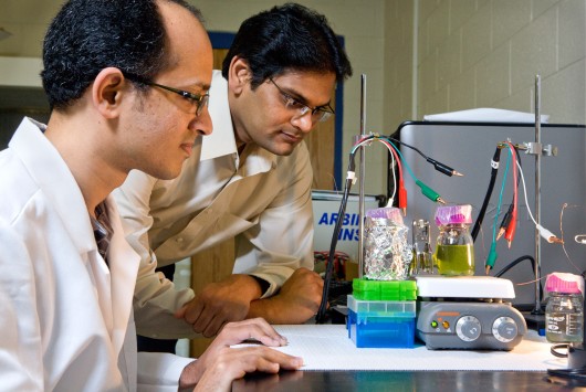
")


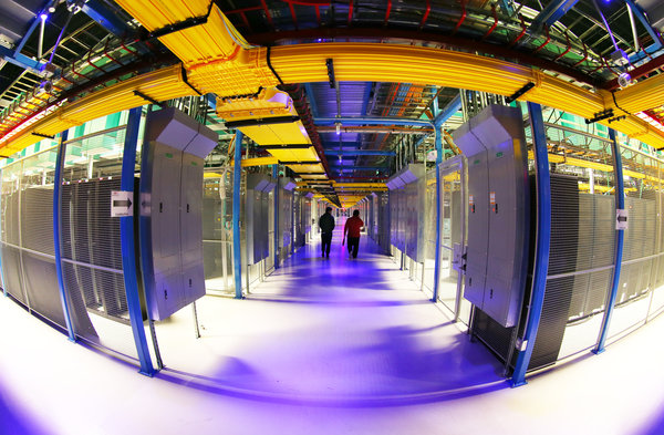
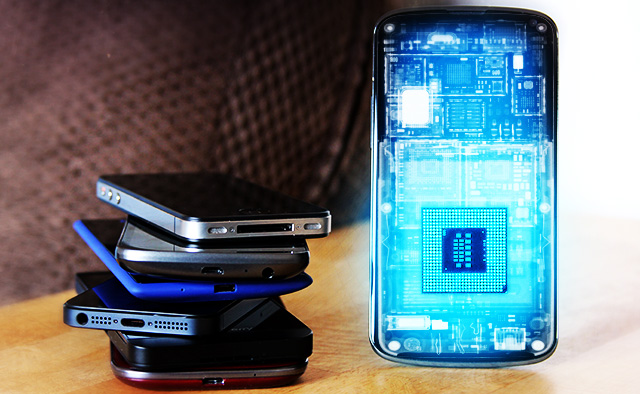
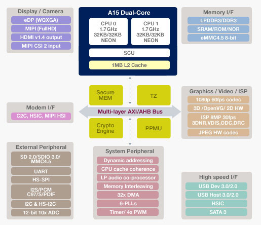

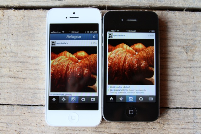

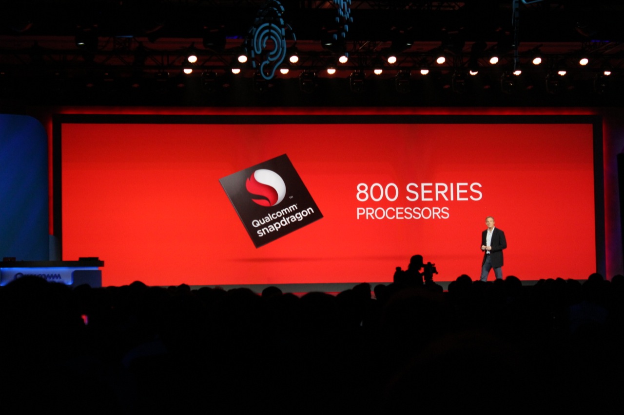
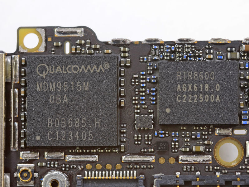
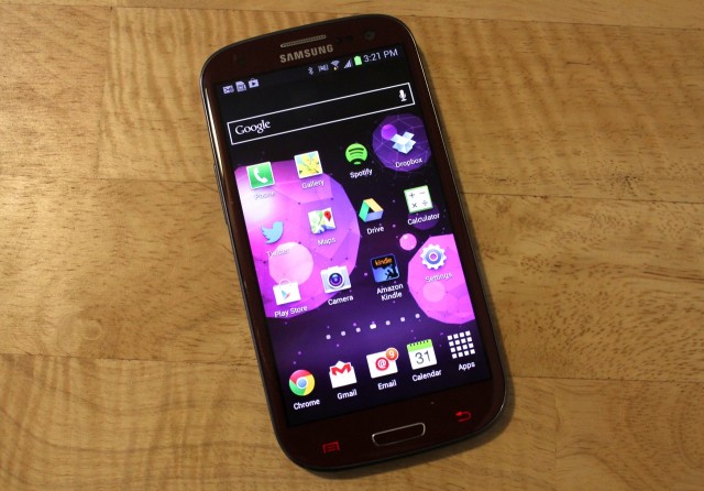
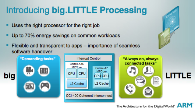
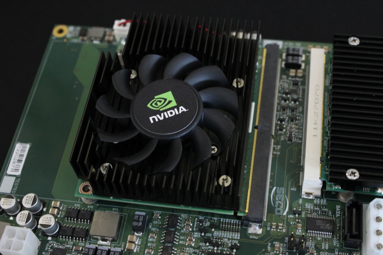
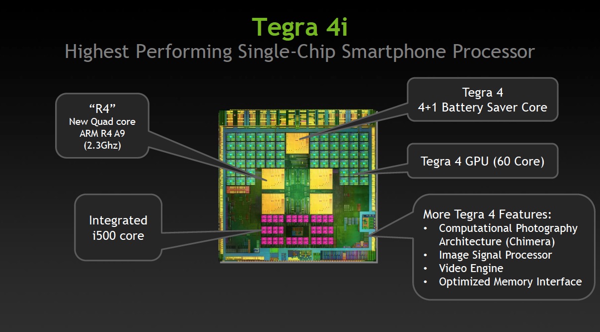
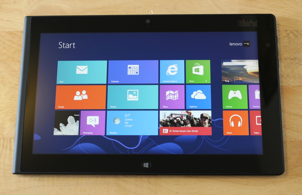
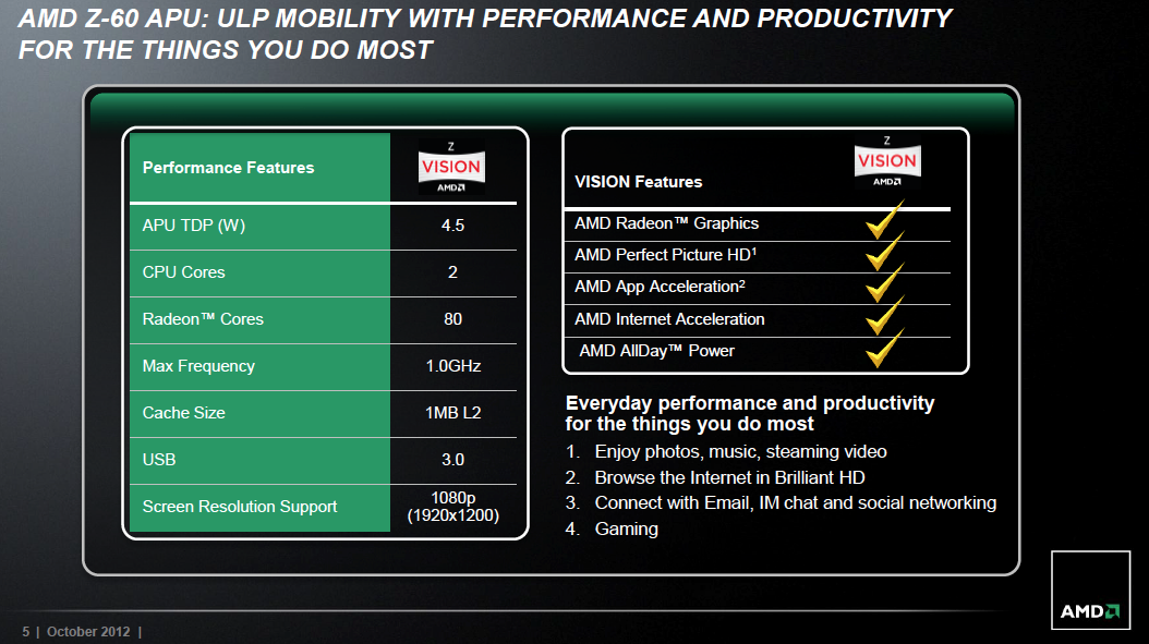

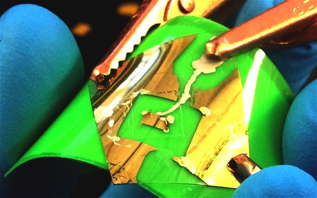
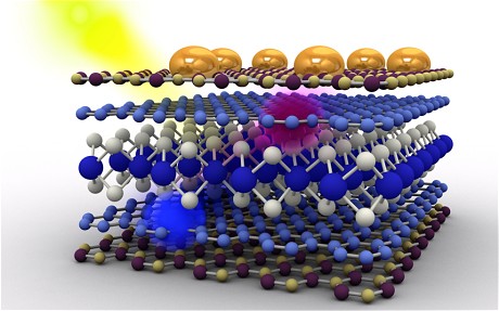

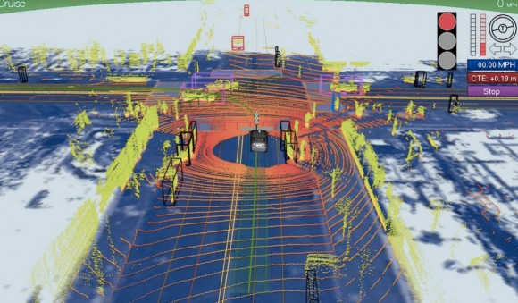

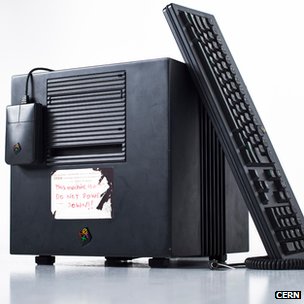
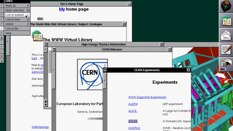
