About BeagleBoard.org and the BeagleBoard.org Foundation
The BeagleBoard.org Foundation is a US-based non-profit corporation
existing to provide education in and
promotion of the design and use of open-source software and hardware in embedded
computing. BeagleBoard.org provides a forum for the owners and
developers of open-source software and hardware to
exchange ideas, knowledge and experience. The BeagleBoard.org community collaborates on
the development of open source physical computing solutions including robotics, personal
manufacturing tools like 3D printers and laser cutters, and other types of industrial
and machine controls.
BeagleBoard.org is the result of an effort by a collection of passionate
individuals, including several employees of Texas Instruments, interested in
creating powerful, open, and embedded devices. We invite you to participate
and become part of BeagleBoard.org, defining its direction.
Support for BeagleBoard.org boards comes from the very active development
community through this website, the mailing list, and the IRC channel.
Original production funding was provided by
Digi-Key, a major international distributor, but distribution has now
been opened up to dozens of distributors across the world. On-going funding
for board prototypes has been provided by manufacturing partners. Texas
Instruments generously allows Jason Kridner, community manager
and software cat herder, to spend time
to provide support and development of the BeagleBoard.org project as part of
their duties at TI. Manufacturing partners pay volume prices for the TI (and all other)
components. BeagleBoard.org licenses the use of BeagleBoard.org logos
for use as part of the Manufacturer, Compliant and
Compatible logo programs
. BeagleBoard.org also participates as a mentoring
organization for Google Summer of Code
which pays a small fee for mentoring
students. The first five BeagleBoard.org designs (BeagleBoard, BeagleBoard-xM,
BeagleBone, BeagleBone Black and BeagleBoard-X15) where all executed by
BeagleBoard.org co-founder Gerald Coley of EmProDesign.
All the designs are fully open source and components are
available for anyone to manufacture compatible hardware. We do request
contact and permission before considering the use of the BeagleBoard.org
name on any products.
The boards are low-cost, fan-less single-board computers based on low-power
Texas Instruments processors featuring the ARM Cortex-A series core with
all of the expandability of today's desktop machines, but without the bulk,
expense, or noise. Initially, development was targeted at enabling Linux
distributions to improve support for ARM devices. With tremendous success
and support by numerous Linux distributions, development has become more
focused on enabling simplified physical computing on advanced GUI-enabled
and/or networked-enabled devices with a super-simple out-of-box learning
experience and support for development environments familiar to just about
every developer, from Ubuntu, QNX, Windows Embedded, Android and web tools
to bare metal and even Arduino/Wiring-style programming.
The ideal 3D bioprinter, says tissue engineering expert Y. Shrike Zhang,
would resemble a breadmaker: “You’d have a few buttons on top, and
you’d press a button to choose heart tissue or liver tissue.” Then Zhang
would walk away from the machine while it laid down complex layers of
cells and other materials.
The technology isn’t quite there yet. But the new BioBot 2 printer
seems a step in that direction. The tabletop device includes a suite of
new features designed to give users easy control over a powerful
device, including automated calibration; six print heads to extrude six
different bioinks; placement of materials with 1-micrometer precision on
the x, y, and z axes; and a user-friendly software interface that
manages the printing process from beginning to end.
BioBots cofounder and CEO Danny Cabrera says the BioBot 2’s features are a result of collaboration with researchers who work in tissue engineering.
“We’ve been working closely with scientists over the past year and a
half to understand what they need to push this work forward,” he says.
“What we found is that they needed more than just a bioprinter—and we
had to do more than just develop a new robot.”
The company’s cloud-based software makes it easy for users to upload
their printing parameters, which the system translates into protocols
for the machine. After the tissue is printed, the system can use
embedded cameras and computer-vision software to run basic analyses. For
example, it can count the number of living versus dead cells in a
printed tissue, or measure the length of axons in printed neurons. “This
platform lets them measure how different printing parameters, like
pressure or cellular resolution, affect the biology of the tissue,”
Cabrera says.
The BioBot 1 hit the
market in 2015 and sells for US $10,000. The company is now taking
orders for the $40,000 BioBot 2, and plans to ship later this year.
Photo: Danny Cabrera
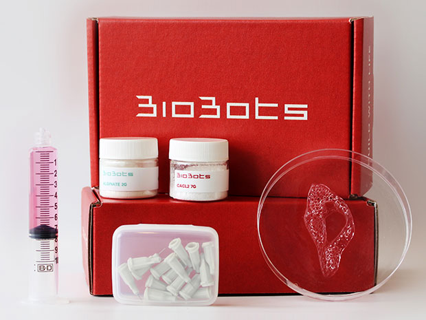
BioBots will soon begin selling a kit with all the materials necessary to print soft tissue, such as cartilage.
Each of the BioBot 2’s print heads can cool its bioink to 4 degrees
Celsius or heat it to 200 degrees Celsius. The printbed is also
temperature-controlled, and it’s equipped with visible and ultraviolet
lights that trigger cross-linking in materials to give make printed
forms more solid.
Cabrera says the temperature controls make it easier to print
collagen, a principal component of connective tissue and bone, because
it cross-links at colder temperatures. “A lot of people were hacking
their bioprinters to get collagen to print,” Cabrera says. “Some were
printing in the refrigerator.”
While some researchers won’t be interested in using the six print
heads to make tissue composed of six different materials, Cabrera says
the design also allows researchers to multiplex experiments. For
example, if researchers are experimenting with the concentration of
cells in a bioink, this setup allows them to simultaneously test six
different versions. “That can save weeks if you have to wait for your
cells to grow after each experiment,” Cabrera says.
And the machine can deposit materials not only on a petri dish, but
also into a cell-culture plate with many small wells. With a 96-well
plate, “you could have 96 lilttle experiments,” says Cabrera.
Photo: Danny Cabrera
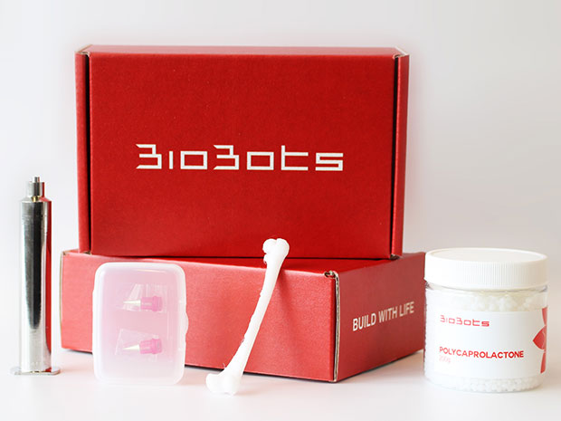
Another kit will include the materials needed to print bone and other hard tissue.
One long-term goal of bioprinting is to give doctors the ability to
press a button and print out a sheet of skin for a burn patient, or a
precisely shaped bone graft for someone who’s had a disfiguring
accident. Such things have been achieved in the lab, but they’re far
from gaining regulatory approval. An even longer-term goal is to give
doctors the power to print out entire replacement organs, thus ending
the shortage of organs available for transplant, but that’s still in the
realm of sci-fi.
While we wait for those applications, however, 3D bioprinters are already finding plenty of uses in biomedical research.
Zhang experimented with an early beta version of the BioBot 1 while working in the Harvard Medical School lab of Ali Khademhosseini.
He used bioprinters to create organ-on-a-chip structures, which mimic
the essential nature of organs like hearts, livers, and blood vessels
with layers of the appropriate cell types laid down in careful patterns.
These small chips can be used for drug screening and basic medical
research. With the BioBot beta, Zhang made a “thrombosis-on-a-chip” where blood clots formed inside miniature blood vessels.
Now an instructor of medicine and an associate bioengineer at Brigham
and Women’s Hospital in Boston, Zhang says he’s intrigued by the BioBot
2. Its ability to print with multiple materials is enticing, he says,
because he wants to reproduce complex tissues composed of different cell
types. But he hasn’t decided yet whether he’ll order one. Like so much
in science, “it depends on funding,” he says.
The BioBot 2 is on the cheaper end of the bioprinter market.
The top-notch machines used by researchers who want nanometer-scale precision typically cost around $200,000—like the large 3D-Bioplotter
from EnvisionTec. This machine was used in research announced just
today, in which Northwestern University scientists 3D-printed a
structure that resembled a mouse ovary. When they seeded it with immature egg cells and implanted it into a mouse, the animal gave birth to live pups.
Photo: Cellink
But there are a few other bioprinters that compete with the BioBot
machines on price. Most notably, a Swedish company called Cellink sells three desktop-sized bioprinters that range in price from $10,000 to $40,000.
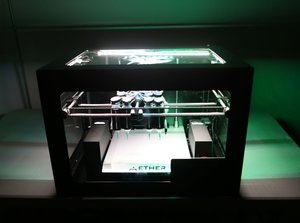
And a San Francisco startup called Aether just recently began sending beta units to researchers for testing and feedback; the company has promised to begin selling its Aether 1 this year for only $9000.
Photo: Aether
The biggest source of competition may not be other companies, but
bioengineers’ innate propensity for tinkering. “We’ll often get some
basic sort of printer and make our own print heads and bioinks,” Zhang
says.
But for biology researchers who don’t have an engineering background,
Zhang says, the BioBot 2 would provide a powerful boost in abilities.
It would be almost like giving a kitchen-phobic individual the sudden
capacity to bake a perfect loaf of whole wheat bread.
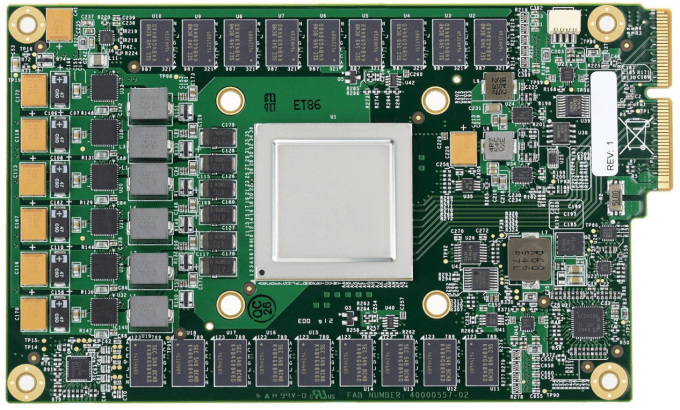
It’s no secret
that Google has developed its own custom chips to accelerate its
machine learning algorithms. The company first revealed those chips,
called Tensor Processing Units (TPUs), at its I/O developer conference
back in May 2016, but it never went into all that many details about
them, except for saying that they were optimized around the company’s
own TensorFlow machine-learning framework. Today, for the first time, it’s sharing more details and benchmarks about the project.
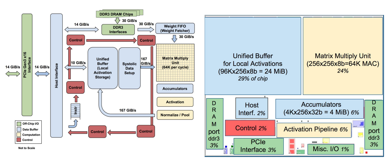
If you’re a chip designer, you can find all the gory glorious details of how the TPU works in Google’s paper.
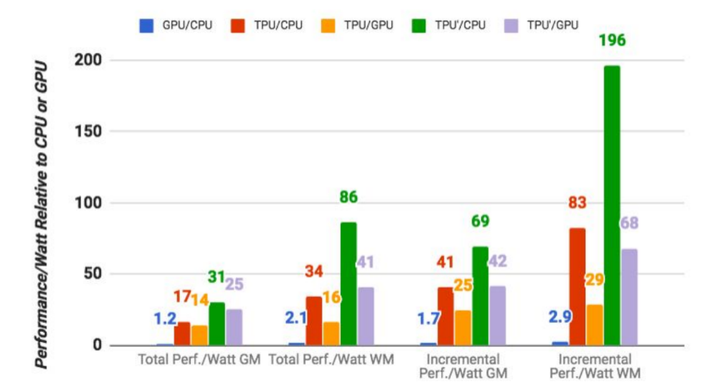
The numbers that matter most here, though, are that based on Google’s
own benchmarks (and it’s worth keeping in mind that this is Google
evaluating its own chip), the TPUs are on average 15x to 30x faster in
executing Google’s regular machine learning workloads than a standard
GPU/CPU combination (in this case, Intel Haswell processors and Nvidia
K80 GPUs). And because power consumption counts in a data center, the
TPUs also offer 30x to 80x higher TeraOps/Watt (and with using faster
memory in the future, those numbers will probably increase).
It’s worth noting that these numbers are about using machine learning
models in production, by the way — not about creating the model in the
first place.
Google also notes that while most architects optimize their chips for convolutional neural networks
(a specific type of neural network that works well for image
recognition, for example). Google, however, says, those networks only
account for about 5 percent of its own data center workload while the
majority of its applications use multi-layer perceptrons.
Google says it started looking into how it could use GPUs, FPGAs and
custom ASICS (which is essentially what the TPUs are) in its data
centers back in 2006. At the time, though, there weren’t all that many
applications that could really benefit from this special hardware
because most of the heavy workloads they required could just make use of
the excess hardware that was already available in the data center
anyway. “The conversation changed in 2013 when we projected that DNNs
could become so popular that they might double computation demands on
our data centers, which would be very expensive to satisfy with
conventional CPUs,” the authors of Google’s paper write. “Thus, we
started a high-priority project to quickly produce a custom ASIC for
inference (and bought off-the-shelf GPUs for training).” The goal here,
Google’s researchers say, “was to improve cost-performance by 10x over
GPUs.”
Google isn’t likely to make the TPUs available outside of its own
cloud, but the company notes that it expects that others will take what
it has learned and “build successors that will raise the bar even
higher.”
Samsung has scrapped its Raspberry Pi 3 competitor called Artik 10 as it moves to smaller and more powerful boards to create gadgets, robots, drones, and IoT devices.
A last remaining stock of the US$149 boards is still available through online retailers Digi-Key and Arrow.
Samsung has stopped making Artik 10 and is asking users to buy its Artik 7 boards instead.
"New development for high-performance IoT products should be based on the Samsung Artik 710, as the Artik 1020 is no longer in production. Limited stocks of Artik 1020 modules and developer kits are still available for experimentation and small-scale projects," the company said on its Artik website.
The Artik boards have been used to develop robots, drone, smart lighting systems, and other smart home products. Samsung has a grand plan to make all its appliances, including refrigerators and washing machines, smart in the coming years, and Artik is a big part of that strategy.
Samsung hopes that tinkerers will make devices that work with its smart appliances. Artik can also be programmed to work with Amazon Echo.
Artik 10 started shipping in May last year, and out-performed Raspberry Pi 3 in many ways, but also lagged on some features.
The board had a plethora of wireless connectivity features including 802.11b/g/n Wi-Fi, Zigbee, and Bluetooth, and it had a better graphics processor than Raspberry Pi. The Artik 10 had 16GB flash storage and 2GB of RAM, both more than Raspberry Pi 3.
The board's biggest flaw was a 32-bit eight-core ARM processor; Raspberry Pi had a 64-bit ARM processor.
The Artik 7 is smaller and a worthy replacement. It has an eight-core 64-bit ARM processor, and it also has Wi-Fi, Bluetooth, and ZigBee. It supports 1080p graphics, and it has 1GB of RAM and 4GB of flash storage, less than in Artik 10. Cameras and sensors can be easily attached to the board.
The Artik boards work on Linux and Tizen. The company also sells Artik 5 and Artik 0, which are smaller boards with lower power processors.
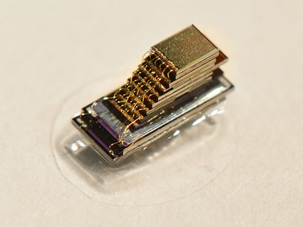
Photo: University of Michigan and TSMC
One of several varieties of University of Michigan micromotes. This one incorporates 1 megabyte of flash memory.
Computer scientist David Blaauw
pulls a small plastic box from his bag. He carefully uses his
fingernail to pick up the tiny black speck inside and place it on the
hotel café table. At 1 cubic millimeter, this is one of a line of the
world’s smallest computers. I had to be careful not to cough or sneeze
lest it blow away and be swept into the trash.
Blaauw and his colleague Dennis Sylvester,
both IEEE Fellows and computer scientists at the University of
Michigan, were in San Francisco this week to present 10 papers related
to these “micromote” computers at the IEEE International Solid-State Circuits Conference (ISSCC). They’ve been presenting different variations on the tiny devices for a few years.
Their broader goal is to make smarter, smaller sensors for medical
devices and the Internet of Things—sensors that can do more with less
energy. Many of the microphones, cameras, and other sensors that make up
the eyes and ears of smart devices are always on alert, and frequently
beam personal data into the cloud because they can’t analyze it
themselves. Some have predicted that by 2035, there will be 1 trillion such devices.
“If you’ve got a trillion devices producing readings constantly, we’re
going to drown in data,” says Blaauw. By developing tiny,
energy-efficient computing sensors that can do analysis on board, Blaauw
and Sylvester hope to make these devices more secure, while also saving
energy.
At the conference, they described micromote designs that use only a
few nanowatts of power to perform tasks such as distinguishing the sound
of a passing car and measuring temperature and light levels. They
showed off a compact radio that can send data from the small computers
to receivers 20 meters away—a considerable boost compared to the
50-centimeter range they reported last year at ISSCC. They also described their work with TSMC
(Taiwan Semiconductor Manufacturing Company) on embedding flash memory
into the devices, and a project to bring on board dedicated, low-power
hardware for running artificial intelligence algorithms called deep
neural networks.
Blaauw and Sylvester say they take a holistic approach to adding new
features without ramping up power consumption. “There’s no one answer”
to how the group does it, says Sylvester. If anything, it’s “smart
circuit design,” Blaauw adds. (They pass ideas back and forth rapidly,
not finishing each other’s sentences but something close to it.)
The memory research is a good example of how the right trade-offs can
improve performance, says Sylvester. Previous versions of the
micromotes used 8 kilobytes of SRAM (static RAM), which makes for a
pretty low-performance computer. To record video and sound, the tiny
computers need more memory. So the group worked with TSMC to bring flash
memory on board. Now they can make tiny computers with 1 megabyte of
storage.
Flash can store more data in a smaller footprint than SRAM, but it
takes a big burst of power to write to the memory. With TSMC, the group
designed a new memory array that uses a more efficient charge pump for
the writing process. The memory arrays are a bit less dense than TSMC’s
commercial products, for example, but still much better than SRAM. “We
were able to get huge gains with small trade-offs,” says Sylvester.
Another micromote they presented at the ISSCC incorporates a deep-learning
processor that can operate a neural network while using just 288
microwatts. Neural networks are artificial intelligence algorithms that
perform well at tasks such as face and voice recognition. They typically
demand both large memory banks and intense processing power, and so
they’re usually run on banks of servers often powered by advanced GPUs.
Some researchers have been trying to lessen the size and power demands
of deep-learning AI with dedicated hardware that’s specially designed to
run these algorithms. But even those processors still use over 50
milliwatts of power—far too much for a micromote. The Michigan group
brought down the power requirements by redesigning the chip
architecture, for example by situating four processing elements within
the memory (in this case, SRAM) to minimize data movement.
The idea is to bring neural networks to the Internet of Things. “A
lot of motion detection cameras take pictures of branches moving in the
wind—that’s not very helpful,” says Blaauw. Security cameras and other
connected devices are not smart enough to tell the difference between a
burglar and a tree, so they waste energy sending uninteresting footage
to the cloud for analysis. Onboard deep-learning processors could make
better decisions, but only if they don’t use too much power. The
Michigan group imagine that deep-learning processors could be integrated
into many other Internet-connected things besides security systems. For
example, an HVAC system could decide to turn the air-conditioning down
if it sees multiple people putting on their coats.
After demonstrating many variations on these micromotes in an
academic setting, the Michigan group hopes they will be ready for market
in a few years. Blaauw and Sylvester say their startup company, CubeWorks,
is currently prototyping devices and researching markets. The company
was quietly incorporated in late 2013. Last October, Intel Capital announced they had invested an undisclosed amount in the tiny computer company.
We invariably imagine electronic devices to be made from silicon
chips, with which computers store and process information as binary
digits (zeros and ones) represented by tiny electrical charges. But it
need not be this way: among the alternatives to silicon are organic
mediums such as DNA.
DNA computing was first demonstrated in 1994 by Leonard Adleman who encoded and solved the travelling salesman problem, a maths problem to find the most efficient route for a salesman to take between hypothetical cities, entirely in DNA.
Deoxyribonucleaic acid, DNA, can store vast amounts of information
encoded as sequences of the molecules, known as nucleotides, cytosine
(C), guanine (G), adenine (A), or thymine (T). The complexity and
enormous variance of different species’ genetic codes demonstrates how
much information can be stored within DNA encoded using CGAT, and this
capacity can be put to use in computing. DNA molecules can be used to
process information, using a bonding process between DNA pairs known as
hybridisation. This takes single strands of DNA as input and produces
subsequent strands of DNA through transformation as output.
Since Adleman’s experiment, many DNA-based “circuits” have been proposed that implement computational methods such as Boolean logic, arithmetical formulas, and neural network computation. Called molecular programming, this approach applies concepts and designs customary to computing to nano-scale approaches appropriate for working with DNA.
It’s circuitry, but not as we know it. Caltech/Lulu Qian, CC BY
In this sense “programming” is really biochemistry. The “programs”
created are in fact methods of selecting molecules that interact in a
way that achieves a specific result through the process of DNA
self-assembly, where disordered collections of molecules will
spontaneously interact to form the desired arrangement of strands of
DNA.
DNA ‘Robots’
DNA can also be used to control motion, allowing for DNA-based nano-mechanical devices. This was first achieved by Bernard Yurke and colleagues in 2000, who created from DNA strands a pair of tweezers that opened and pinched. Later experiments such as by Shelley Wickham and colleagues in 2011 and at Andrew Turberfield’s lab at Oxford demonstrated nano-molecular walking machines made entirely from DNA that could traverse set routes.
One possible application is that such a nano-robot DNA walker could
progress along tracks making decisions and signal when reaching the end
of the track, indicating computation has finished. Just as electronic
circuits are printed onto circuit boards, DNA molecules could be used to
print similar tracks arranged into logical decision trees on a DNA
tile, with enzymes used to control the decision branching along the
tree, causing the walker to take one track or another.
DNA molecules’ many appealing features include their size (2nm
width), programmability and high storage capacity – much greater than
their silicon counterparts. DNA is also versatile, cheap and easy to
synthesise, and computing with DNA requires much less energy than
electric powered silicon processors.
Its drawback is speed: it currently takes several hours to compute
the square root of a four digit number, something that a traditional
computer could compute in a hundredth of a second. Another drawback is
that DNA circuits are single-use, and need to be recreated to run the
same computation again.
Perhaps the greatest advantage of DNA over electronic circuits is
that it can interact with its biochemical environment. Computing with
molecules involves recognising the presence or absence of certain
molecules, and so a natural application of DNA computing is to bring
such programmability into the realm of environmental biosensing, or
delivering medicines and therapies inside living organisms.
DNA programs have already been put to medical uses, such as diagnosing tuberculosis. Another proposed use is a nano-biological “program” by Ehud Shapiro of the Weizmann Institute of Science in Israel, termed the “doctor in the cell”
that targets cancer molecules. Other DNA programs for medical
applications target lymphocytes (a type of white blood cell), which are
defined by the presence or absence of certain cell markers and so can be
naturally detected with true/false Boolean logic. However, more effort
is required before we can inject smart drugs directly into living organisms.
Future of DNA Computing
Taken broadly, DNA computation has enormous future potential. Its
huge storage capacity, low energy cost, ease of manufacturing that
exploits the power of self-assembly and its easy affinity with the
natural world are an entry to nanoscale computing, possibly through
designs that incorporate both molecular and electronic components. Since
its inception, the technology has progressed at great speed, delivering
point-of-care diagnostics and proof-of-concept smart drugs – those that
can make diagnostic decisions about the type of therapy to deliver.
There are many challenges, of course, that need to be addressed so
that the technology can move forward from the proof-of-concept to real
smart drugs: the reliability of the DNA walkers, the robustness of DNA
self-assembly, and improving drug delivery. But a century of traditional
computer science research is well placed to contribute to developing
DNA computing through new programming languages, abstractions, and
formal verification techniques – techniques that have already
revolutionised silicon circuit design, and can help launch organic
computing down the same path.
While companies like Facebook have been relatively open
about their data center networking infrastructure, Google has
generally kept pretty quiet about how it connects the thousands of
servers inside its data centers to each other (with a fewexceptions). Today, however, the company revealed a bit more about the technology that lets its servers talk to each other.
It’s no secret that Google often builds its own custom hardware for
its data centers, but what’s probably less known is that Google uses
custom networking protocols that have been tweaked for use in its data
centers instead of relying on standard Internet protocols to power its
networks.
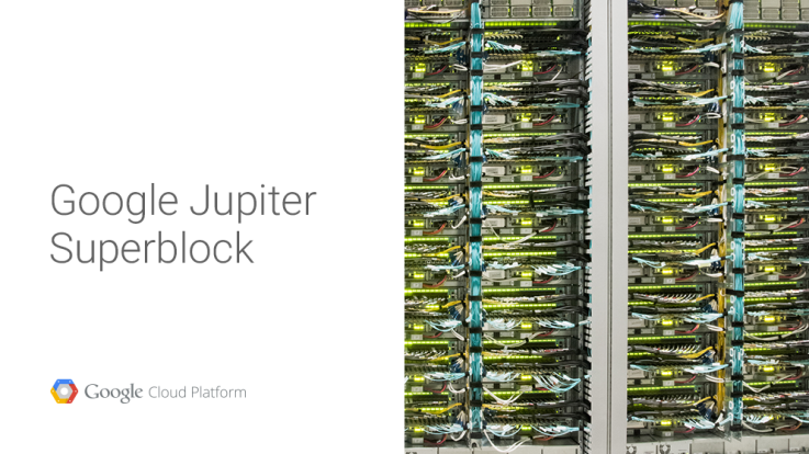
Google says its current ‘Jupiter’ networking setup — which represents
the fifth generation of the company’s efforts in this area — offers
100x the capacity of its first in-house data center network. The current
generation delivers 1 Petabit per second of bisection bandwidth (that
is, the bandwidth between two parts of the network). That’s enough to allow 100,000 servers to talk to each other at 10GB/s each.
Google’s technical lead for networking, Amin Vahdat, notes that the
overall network control stack “has more in common with Google’s
distributed computing architectures than traditional router-centric
Internet protocols.”
Here is how he describes the three key principles behind the design of Google’s data center networks:
We arrange our network around a Clos topology,
a network configuration where a collection of smaller (cheaper)
switches are arranged to provide the properties of a much larger logical
switch.
We use a centralized software control stack to manage
thousands of switches within the data center, making them effectively
act as one large fabric.
We build our own software and hardware using silicon from
vendors, relying less on standard Internet protocols and more on custom
protocols tailored to the data center.
Sadly, there isn’t all that much detail here — especially compared to some of the information
Facebook has shared in the past. Hopefully Google will release a bit
more in the months to come. It would be especially interesting to see
how its own networking protocols work and hopefully the company will
publish a paper or two about this at some point.
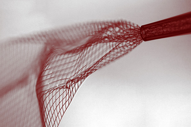
Above:
Bright-field image showing the mesh electronics being injected through
sub-100 micrometer inner diameter glass needle into aqueous solution.
(Lieber Research Group/Harvard University
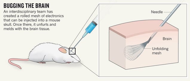
Harvard scientists have developed an electrical scaffold that can be
injected directly into the brain with a syringe. By using the technique
to “cyborg”-ize the brains of mice, the team was able to investigate and
manipulate the animals’ individual neurons—a technological feat the
researchers say holds tremendous medical promise.
As reported in Nature News,
the soft, conductive polymer mesh can be injected into a mouse’s brain,
where it unfurls and takes root. And because the mesh can be laced with
tiny electronic devices, the implant can be custom-designed to perform a
number of tasks, from monitoring brain activity to stimulating brain
functions. Once proven safe, the technology could be applied in humans,
where it could be used to treat Parkinson’s, among other cognitive
disorders. The details of this research, led by Harvard’s Charles
Lieber, can be found in the journal Nature Nanotechnology.
“I do feel that this has the potential to be revolutionary,” Lieber noted in a Harvard statement.
“This opens up a completely new frontier where we can explore the
interface between electronic structures and biology. For the past 30
years, people have made incremental improvements in micro-fabrication
techniques that have allowed us to make rigid probes smaller and
smaller, but no one has addressed this issue — the electronics/cellular
interface — at the level at which biology works.”
(Credit: Nature News/Nature Nanotechnology/Lieber Research Group/Harvard University)
Nature News’s Elizabeth Gibney explains how it works:
"The
Harvard team [used] a mesh of conductive polymer threads with either
nanoscale electrodes or transistors attached at their intersections.
Each strand is as soft as silk and as flexible as brain tissue itself.
Free space makes up 95% of the mesh, allowing cells to arrange
themselves around it.
In
2012, the team showed that living cells grown in a dish can be coaxed
to grow around these flexible scaffolds and meld with them, but this
‘cyborg’ tissue was created outside a living body. “The problem is, how
do you get that into an existing brain?” says Lieber.
The
team’s answer was to tightly roll up a 2D mesh a few centimetres wide
and then use a needle just 100 micrometres in diameter to inject it
directly into a target region through a hole in the top of the skull.
The mesh unrolls to fill any small cavities and mingles with the tissue.
Nanowires that poke out can be connected to a computer to take
recordings and stimulate cells."
Using this
technique, the researchers implanted meshes consisting of 16 electric
elements into two different brain regions, enabling them to monitor and
stimulate individual neurons. The researchers would like to scale up to
hundreds of devices outfitted with different kinds of sensors. In the
future, these arrays might be used to treat motor disorders, paralysis,
and repair brain damage caused by stroke. What’s more, these implants
could conceivably be used in other parts of the body. But before they
get too carried away, the researchers will have to prove that the
implantable technology is safe in the longterm.
Technology giant IBM announced two major breakthroughs
towards the building of a practical quantum computer, the next evolution
in computing that will be required as Moore’s Law runs out of steam.
Described in the April 29 issue of the journal Nature Communications,
the breakthroughs include the ability to detect and measure both kinds
of quantum errors simultaneously and a new kind of circuit design, which
the company claims is "the only physical architecture that could
successfully scale to larger dimensions."
The two innovations are interrelated: The quantum bit
circuit, based on a square lattice of four superconducting "qubits" --
short for quantum bits -- on a chip roughly one-quarter-inch square,
enables both types of quantum errors to be detected at the same time.
(Image courtesy of IBM)
The IBM project, which was funded in part by the
Intelligence Advanced Research Projects Activity (IARPA) Multi-Qubit
Coherent Operations program, opts for a square-shaped design as opposed
to a linear array, which IBM said prevents the detection of both kinds
of quantum errors simultaneously.
Jerry M. Chow, manager of the Experimental Quantum Computing
group at IBM’s T.J. Watson Research Center, and the primary
investigator on the IARPA-sponsored Multi-Qubit Coherent Operations
project, told InformationWeek that one area they are excited about is
the potential for quantum computers to simulate systems in nature.
"In physics and chemistry, quantum computing will allow us
to design new materials and drug compounds without the expensive
trial-and-error experiments in the lab, dramatically speeding up the
rate and pace of innovation," Chow said. "For instance, the
effectiveness of drugs is governed by the precise nature of the chemical
bonds in the molecules constituting the drug."
He noted the computational chemistry required for many of
these problems is out of the reach of classical computers, and this is
one example of where quantum computers may be capable of solving such
problems leading to better drug design.
The qubits, IBM said, could be designed and manufactured
using standard silicon fabrication techniques, once a handful of
superconducting qubits can be manufactured quickly and reliably, and
boast low error-rates.
"Quantum information is very fragile, requiring the quantum
elements to be cooled to near absolute zero temperature and shielded
from its environment to minimize errors," Chow explained. "A quantum
bit, the component that carries information in a quantum system, can be
susceptible to two types of errors -- bit-flip and phase-flip. It either
error occurs, the information is destroyed and it cannot carry out the
operation."
He said it is important to detect and measure both types of
errors in order to know what errors are present and how to address them,
noting no one has been able to do this before in a scalable
architecture.
"We are at the stage of figuring out the building blocks of
quantum computers -- a new paradigm of computing completely different
than how computers are built today," Wong said. "In the arc of quantum
computing progress, we are at the moment of time similar to when
scientists were building the first transistor. If built, quantum
computers have the potential to unlock new applications for scientific
discovery and data analysis and will be more powerful than any
supercomputer today."
Remember when the Internet was just that thing you accessed on your computer?
Today, connectivity is popping up in some surprising places: kitchen
appliances, bathroom scales, door locks, clothes, water bottles… even
toothbrushes.
That’s right, toothbrushes. The Oral-B SmartSeries is billed as the
world’s first “interactive electric toothbrush” with built-in Bluetooth.
Whatever your feelings on this level of connectivity, it’s undeniable
that it’s a new frontier for data.
And let’s face it, we’re figuring it out as we go. Consequently, it’s
a good idea to keep your devices secure - and that means leveraging a
product like Norton Security,
which protects mobile devices and can help keep intruders out of your
home network. Because, let’s face it, the last thing you want is a
toothbrush that turns on you.
Welcome to the age of the Internet of Things (IoT for short), the
idea that everyday objects - and everyday users - can benefit from
integrated network connectivity, whether it’s a washing machine that
notifies you when it’s done or a collar-powered tracker that helps you
locate your runaway pet.
Some of these innovations are downright brilliant. Others veer into
impractical or even unbelievable. And some can present risks that we’ve
never had to consider before.
Consider the smart lock. A variety of companies offer deadbolt-style
door locks you can control from your smartphone. One of them, the August Smart Lock,
will automatically sense when you approach your door and unlock it for
you, even going so far as to lock it again once you’ve passed through.
And the August app not only logs who has entered and exited, but also
lets you provide a temporary virtual key to friends, family members, a
maid service, and the like.
That’s pretty cool, but what happens in the event of a dead battery -
either in the user’s smartphone or the lock itself? If your phone gets
lost or stolen, is there a risk a thief can now enter your home? Could a
hacker “pick” your digital lock? Smart lock-makers promise safeguards
against all these contingencies, but it begs the question whether the
conveniences outweigh the risks. Do we really need the Internet in all
our things?
The latest that-can’t-possibly-be-a-real-product example made its debut at this year’s Consumer Electronics Show: The Belty,
an automated belt/buckle combo that automatically loosens when you sit
and tightens when you stand. A smartphone app lets you control the
degree of each. Yep.
Then there’s the water bottle that reminds you to drink more water.
The smart exercise shirt your trainer can use to keep tabs on your
activity (or lack thereof). And who can forget the HAPIfork, the “smart”
utensil that aims to steer you toward healthier eating by reminding you
to eat more slowly?
Stop the Internet (of Things), I want to get off.
Okay, I shouldn’t judge. And it’s not all bad. There is real value in - and good reason to be excited about - a smart basketball that helps you perfect your jump shot. Or a system of smart light bulbs designed to deter break-ins. Ultimately, the free market will decide which ones are useful and which ones are ludicrous.
The important thing to remember is that with the IoT, we’re venturing
into new territory. We’re linking more devices than ever to our home
networks. We’re installing phone and tablet apps that have a direct line
not just to our data, but also our very domiciles.