Tuesday, July 02. 2013
Exploring the Floating Point Performance of Modern ARM Processors
Via ANANDTECH
-----
As a programmer who wants to write decent performing code, I am very
interested in understanding the architectures of CPUs and GPUs. However,
unlike desktop and server CPUs, mobile CPU and GPU vendors tend to do
very little architectural disclosure - a fact that we've been working
hard to change over the past few years. Often times all that's available
are marketing slides with fuzzy performance claims. This situation
frustrates me to no end personally. We've done quite a bit of low-level
mobile CPU analysis at AnandTech in pursuit of understanding
architectures where there is no publicly available documentation. In
this spirit, I wrote a few synthetic tests to better understand the
performance of current-gen ARM CPU cores without having to rely upon
vendor supplied information. For this article I'm focusing exclusively
on floating point performance.
We will look at 5 CPU cores today: the ARM Cortex A9, ARM Cortex A15,
Qualcomm Scorpion, Qualcomm Krait 200 and Qualcomm Krait 300. The test
devices are listed below.
| Device | OS | SoC | CPU | Frequency | Number of cores |
| Samsung Galaxy SIIX (T989D) | Android 4.0 | Qualcomm APQ8060 | Scorpion | 1.5GHz | 2 |
| Boundary devices BD-SL-i.mx6 | Ubuntu Oneiric | Freescale i.mx6 | Cortex-A9 | 1.0GHz | 4 |
| Blackberry Z10 | Blackberry 10 (10.1) | Qualcomm MSM8960 | Krait 200 | 1.5GHz | 2 |
| Google Nexus 10 | Android 4.2.2 | Samsung Exynos 5250 | Cortex-A15 | 1.7GHz | 2 |
| HTC One | Android 4.1.2 | Qualcomm Snapdragon 600 | Krait 300 | 1.7GHz | 4 |
I wanted to test the instruction throughput of various floating point
instructions. I wrote a simple benchmark consisting of a loop with a
large number of iterations. The loop body consisted of many (say 20)
floating point instructions with no data dependence between them. The
tests were written in C++ with gcc NEON intrisincs where required, and I
always checked the assembler to verify that the generated assembly was
as expected. There were no memory instructions inside the loop and thus
memory performance was not an issue. There were minimal dependencies in
the loop body. I tested the performance of scalar addition,
multiplication and multiply-accumulate for 32-bit and 64-bit floating
point datatypes. All the tested ARM processors also support the NEON
instruction set, which is a SIMD (single instruction multiple data)
instruction set for ARM for integer and floating point operations. I
tested the performance of 128-bit floating point NEON instructions for
addition, multiplication and multiply-accumulate.
Apart from testing throughput of individual instructions, I also wrote a
test for testing throughput of a program consisting of two types of
instructions: scalar addition and scalar multiplication instructions.
The instructions were interleaved, i.e. the program consisted of an
addition followed by a multiply, followed by another add, then another
multiply and so on. There were no dependencies between the additions and
following multiplies. You may be wondering the reasoning behind this
mixed test. Some CPU cores (such as AMD's K10 core) have two floating
point units but the two floating point units may not be identical. For
example, one floating point unit may only support addition while another
may only support multiplication. Thus, if we only test the additions
and multiplications separately, we will not see the peak throughput on
such a machine. We perform the mixed test to identify such cases.
All the tests mentioned above measure the amount of time taken for a
particular number of instructions and thus we get the instructions
executed per-second. We also need to know the frequency to get the
instructions executed per-cycle. Knowing the peak frequency of the
device is not enough because CPUs have multiple frequency states and the
tests may not be running at the advertised peak speeds. Thus, I also
wrote code to monitor the percentage of time spent in each frequency
state as reported by the kernel. The frequency was calculated as the
average of the frequency states weighted by percentage of time spent in
each state. The observed frequency on Scorpion (APQ8060) , Cortex A9
(i.mx6) and Cortex A15 (Exynos 5250) were 1.242 GHz, 992MHz and 1.7GHz
respectively on all tests except where noted in the results below.
However, as it turns out, the method I used for measuring the time
spent in each frequency state does not work on aSMP designs like the
Krait 200 based Snapdragon S4 and Krait 300 based Snapdragon 600. For
Krait 200, the results reported here are for MSM8960 which shouldn't
really have thermal throttling issues. My results on the MSM8960 also
line up quite neatly with the assumption that the CPU spent most or all
of its time in the test in the peak frequency state. Brian also ran the
test on a Nexus 4 and the results were essentially identical as both
have the same peak, which is additional confirmation that our results
are likely correct. Thus I will assume a frequency of 1.5 GHz while
discussing Krait 200 results. Results on Krait 300 (Snapdragon 600)
however are more mixed. I am not sure if it is reaching peak frequency
on all the tests and thus I am less sure of the per-cycle estimates on
this chip. Brian also ran the tests on another handset (LG Optimus G
Pro) with the same Snapdragon 600, and the results were qualitatively
very similar.
Now the results. First up, the raw data collected from the tests in gigaflops:
| |
Scorpion (APQ8060) |
Cortex-A9 (i.mx6) |
Krait 200 (MSM8960) |
Cortex-A15 (Exynos 5250) |
Krait 300 (Snapdragon 600) |
| Add (fp64) | 1.23 | 0.99 | 1.33 | 1.55 @ 1.55 GHz | 1.6 |
| Add (fp32) | 1.19 | 0.99 | 1.46 | 1.69 | 1.72 |
| Mul (fp64) | 0.61 | 0.50 | 1.48 | 1.69 | 1.72 |
| Mul (fp32) | 1.22 | 0.99 | 1.49 | 1.69 | 1.72 |
| Mixed (fp64) | 0.82 | 0.99 | 1.48 | 1.63 | 1.72 |
| Mixed (fp32) | 1.23 | 0.99 | 1.47 | 1.69 | 1.72 |
| MAC (fp64) | 1.23 | 0.99 | 1.48 | 3.35 | 2.65 |
| MAC (fp32) | 2.47 | 1.98 | 1.47 | 3.39 | 3.13 |
| Add (fp32 NEON) | 4.94 | 1.99 | 5.86 | 6.77 | 6.89 |
| Mul (fp32 NEON) | 4.89 | 1.99 | 5.76 | 6.77 | 6.89 |
| MAC (fp32 NEON) | 9.88 | 3.98 | 5.91 | 13.55 | 12.5 |
Before we discuss the results, it is important to keep in mind that the results and per-cycle timing estimates reported are what I observed from the tests. I did my best to ensure that the design of the tests was very conducive to achieving high throughput. However, it is possible there may be some cases where an architecture can achieve higher performance than what what I was able to get out of my tests. With that out of the way, lets look at the results.
In the data, we need to distinguish between number of instructions and number of flops. I count scalar addition and multiply as one flop and scalar MACs as two flops. I count NEON addition and multiply as four flops and NEON MACs are counted as eight flops. Thus, we get the following per-cycle instruction throughput estimates:
| |
Scorpion | Cortex A9 | Krait 200 | Cortex A15 | Krait 300 |
| Add (fp64) | 1 | 1 | 1 | 1 | 1 |
| Add (fp32) | 1 | 1 | 1 | 1 | 1 |
| Mul (fp64) | 1/2 | 1/2 | 1 | 1 | 1 |
| Mul (fp32) | 1 | 1 | 1 | 1 | 1 |
| Mixed (fp64) | 2/3 | 1 | 1 | 1 | 1 |
| Mixed (fp32) | 1 | 1 | 1 | 1 | 1 |
| MAC (fp64) | 1/2 | 1/2 | 1/2 | 1 | 7/9 |
| MAC (fp32) | 1 | 1 | 1/2 | 1 | 10/11 |
| Add (fp32 NEON) | 1 | 1/2 | 1 | 1 | 1 |
| Mul (fp32 NEON) | 1 | 1/2 | 1 | 1 | 1 |
| MAC (fp32 NEON) | 1 | 1/2 | 1/2 | 1 | 10/11 |
We start with the Cortex A9. Cortex A9 achieves throughput of 1 operation/cycle for most scalar instructions, except for fp64 MUL and fp64 MAC, which can only be issued once every two cycles. The mixed test reveals that though fp64 muls can only be issued every two cycles, Cortex A9 can issue a fp64 add in the otherwise empty pipeline slot. Thus, in the mixed test it was able to achieve throughput of 1 instruction/cycle. NEON implementation in Cortex A9 has a 64-bit datapath and all NEON instructions take 2 cycles. Qualcomm's Scorpion implementation of scalar implementations is similar to Cortex A9 except that it seems unable to issue fp64 adds immediately after fp64 muls in the mixed test. Scorpion uses a full 128-bit datapath for NEON and has twice the throughput of Cortex A9.
Krait 200 features an improved multiplier, and offers 1
instruction/cycle throughput for most scalar and NEON instructions.
Interestingly, Krait 200 has half the per-cycle throughput for MAC
instructions, which is a regression compared to Scorpion. Krait 300
improves the MAC throughput compared to Krait 200, but still appears to
be unable to reach throughput of 1 instruction/cycle possibly revealing
some issues in the pipeline. An alternate explanation is that Snapdragon
600 reduced the frequency in the MAC tests for some unknown reason.
Without accurate frequency information, currently it is difficult to
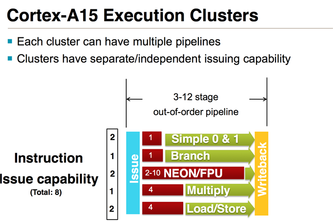
make that judgment. Cortex A15 is the clear leader here, and offers
throughput of 1 FP instruction/cycle in all our tests.
In the big picture, readers may want to know how the the floating point
capabilities of these cores compares to x86 cores. I consider Intel's
Ivy Bridge and Haswell as datapoints for big x86 cores, and AMD Jaguar
as a datapoint for a small x86 core. For double-precision (fp64),
current ARM cores appear to be limited to 2 flops/cycle for FMAC-heavy
workloads and 1 flops/cycle for non-FMAC workloads. Ivy Bridge can have a
throughput of up to 8 flops/cycle and Haswell can do 16 flops/cycle
with AVX2 instructions. Jaguar can execute up to 3 flops/cycle. Thus,
current ARM cores are noticeably behind in this case. Apart from the
usual reasons (power and area constraints, very client focused designs),
current ARM cores also particularly lag behind in this case because
currently NEON does not have vector instructions for fp64. ARMv8 ISA
adds fp64 vector instructions and high performance implementations of
the ISA such as Cortex A57 should begin to reduce the gap.
For fp32, Ivy Bridge can execute up to 16 fp32 flops/cycle, Haswell can
do up to 32 fp32 flops/cycle and AMD's Jaguar can perform 8 fp32
flops/cycle. Current ARM cores can do up to 8 flops/cycle using NEON
instructions. However, ARM NEON instructions are not IEEE 754 compliant,
whereas SSE and AVX floating point instructions are IEEE 754 compliant.
Thus, comparing flops obtained in NEON instructions to SSE instructions
is not apples-to-apples comparison. Applications that require IEEE 754
compliant arithmetic cannot use NEON but more consumer oriented
applications such as multimedia applications should be able to use NEON.
Again, ARMv8 will fix this issue and will bring fully IEEE
754-compliant fp32 vector instructions.
To conclude, Cortex A15 clearly leads amongst the CPUs tested today
with Krait 300 very close behind. It is also somewhat disappointing that
none of the CPU cores tested displayed a throughput of more than 1 FP
instruction/cycle in these tests. I end at a cautionary note that the
tests here are synthetic tests that only stress the FP units. Floating
point ALU peaks are only a part of a microarchitecture. Performance of
real-world applications will depend upon rest of the microarchitecture
such as cache hierarchy, out of order execution capabilities and so on.
We will continue to make further investigations into these CPUs to
understand them better.
Quicksearch
Popular Entries
- The great Ars Android interface shootout (131491)
- Norton cyber crime study offers striking revenue loss statistics (102340)
- MeCam $49 flying camera concept follows you around, streams video to your phone (100502)
- The PC inside your phone: A guide to the system-on-a-chip (58677)
- Norton cyber crime study offers striking revenue loss statistics (58569)
