Via Slash Gear
-----
IBM has
developed a light-based data transfer system delivering more
than 25Gbps per channel, opening the door to chip-dense slabs of
processing power that could speed up server performance, the internet,
and more. The company’s research into silicon integrated nanophotonics addresses
concerns that interconnects between increasingly powerful computers,
such as mainframe servers, are unable to keep up with the speeds of the
computers themselves. Instead of copper or even optical cables, IBM
envisages on-chip optical routing, where light blasts data between
dense, multi-layer computing hubs.

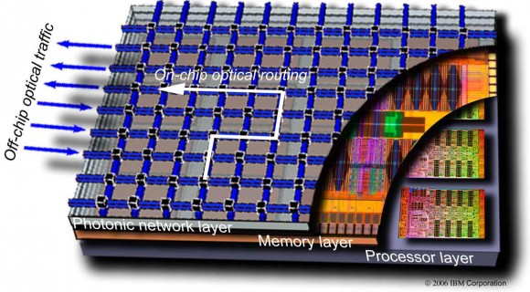
“This future 3D-integated chip consists of several layers
connected with each other with very dense and small pitch interlayer
vias. The lower layer is a processor itself with many hundreds of
individual cores. Memory layer (or layers) are bonded on top to provide
fast access to local caches. On top of the stack is the Photonic layer
with many thousands of individual optical devices (modulators,
detectors, switches) as well as analogue electrical circuits
(amplifiers, drivers, latches, etc.). The key role of a photonic layer
is not only to provide point-to-point broad bandwidth optical link
between different cores and/or the off-chip traffic, but also to route
this traffic with an array of nanophotonic switches. Hence it is named
Intra-chip optical network (ICON)” IBM
Optical interconnects are increasingly being used to link different
server nodes, but by bringing the individual nodes into a single stack
the delays involved in communication could be pared back even further.
Off-chip optical communications would also be supported, to link the
data-rich hubs together.
Although the photonics system would be considerably faster than
existing links – it supports multiplexing, joining multiple 25Gbps+
connections into one cable thanks to light wavelength splitting – IBM
says it would also be cheaper thanks to straightforward manufacturing
integration:
“By adding a few processing modules into a
high-performance 90nm CMOS fabrication line, a variety of silicon
nanophotonics components such as wavelength division multiplexers (WDM),
modulators, and detectors are integrated side-by-side with a CMOS
electrical circuitry. As a result, single-chip optical communications
transceivers can be manufactured in a conventional semiconductor
foundry, providing significant cost reduction over traditional
approaches” IBM
Technologies like the co-developed Thunderbolt from Intel
and Apple have promised affordable light-based computing connections,
but so far rely on more traditional copper-based links with optical
versions further down the line. IBM says its system is “primed for
commercial development” though warns it may take a few years before
products could actually go on sale.

