Friday, August 26. 2011
MicroGen Chips to Power Wireless Sensors Through Environmental Vibrations
Via Daily Tech
-----
MicroGen Systems says its chips differ from other vibrational energy-harvesting devices because they have low manufacturing costs and use nontoxic material instead of PZT, which contains lead.
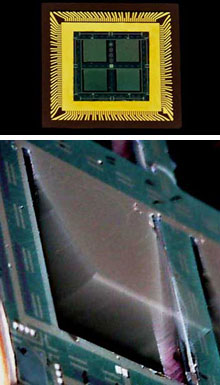
(TOP) Prototype wireless sensor battery with four energy-scavenging chips. (BOTTOM) One chip with a vibrating cantilever (Source: MicroGen Systems )
MicroGen
Systems is in the midst of creating energy-scavenging chips that will convert
environmental vibrations into electricity to power wireless sensors.
The
chip's core consists of an array of small silicon cantilevers that
measure one centimeter squared and are located on a
"postage-stamp-sized" thin film battery. These cantilevers oscillate
when the chip is shook, and at their base is piezoelectric material that produces electrical potential when strained by
vibrations.
The current travels from the piezoelectric array through an electrical device
that converts it to a compatible form for the battery. When jostling the chip
by vibrations of a rotating tire, for example, it can generate 200 microwatts
of power.
Critics such as David Culler, chair of computer science at the University of
California, have said that 200 microwatts may be useful at a small size, but
other harvesting techniques through solar, light, heat, etc. are
more competitive technologies since they can either store the electrical energy
on a battery or use it right away.
But according to Robert Andosca, founder and president of Ithaca, New
York-based MicroGen Systems, his chips differ from other vibrational
energy-harvesting devices because they have low manufacturing costs and use
nontoxic material instead of PZT, which contains lead.
Most piezoelectric materials must be assembled by hand and can be quite large.
But MicroGen's chips can be made inexpensively and small because they are based
on silicon microelectrical mechanical systems. The chips can be made on the
same machines used to make computer chips.
MicroGen Systems hopes to use these energy-harvesting chips to power wireless sensors like those that
monitor tire pressure. The chips could eliminate the need to replace these
batteries.
"It's a pain in the neck to replace those batteries," said Andosca.
MicroGen Systems plans to sell these chips at $1 a piece, depending on the
volume, and hopes to begin selling them in about a year.
Wednesday, August 03. 2011
WIMM Wearable Platform
Via SlashGear
-----
Wearable sub-displays keep coming around, and WIMM Labs is the latest company to try its hand at the segment. Its WIMM Wearable Platform – a 1.4-inch color touchscreen, scaled to be wearable on your wrist, and paired with WiFi, Bluetooth, various sensors and running Android-based “Micro Apps” – obviously stood out of the crowd, having caught the attention of Foxconn and two rounds of financing from the huge manufacturing/ODM company. We caught up with the WIMM Labs team to check out the Wearable Platform and find out if it stood more chance of success than, say, Sony Ericsson’s LiveView.
The basic premise of the Wearable Platform isn’t new. People carry their phones and tablets in pockets and bags, not in their hand, and so when nuggets of information, alerts and updates come in, they need to be taken out in order to check them. A wearable display – strapped to your wrist, hanging on a lanyard from your belt or bag, or otherwise attached to you – means at-a-glance review, allowing you to decide whether you need to fish out your phone or if it can wait until later.

WIMM’s One developer kit hardware is a step ahead of some systems we’ve already seen. The 1.4-inch capacitive touch display operates in dual-modes, either as a regular screen or transflective backlight-free so that it’s still readable (albeit in monochrome) but battery life is extended. This passive display mode works in tandem with a 667MHz Samsung microcontroller, WiFi, Bluetooth, GPS, an accelerometer and a digital compass, all contained in a waterproof casing – made of either plastic or of a new wireless-compatible ceramic – measuring 32 x 36 x 12.5 mm and weighing 22g.

That casing, WIMM says, should be standardized so that each unit – the Wearable Platform will be licensed out to third-party companies – will hopefully be interchangeable with the same mounting pins. That way, if you buy a new model from another firm, it should be able to snap into your existing watch strap. Up to 32GB of memory is supported, and the One can notify you with audio or tactile alerts. Battery life is said to last at least a full day, and it recharges using a magnetic charger (that plugs in via microUSB) or a collapsable desk-stand that adds an integrated battery good for up to four recharge cycles and useful if you’re on the road.

Control is via a series of taps, swipes and physical gestures (the sensors allow the Wearable Platform to react to movement), including a two-finger swipe to pull down the watch face. WIMM will preload a handful of apps – the multifunction clock, a real-time information viewer showing weather, etc, and a cellphone companion which can show incoming caller ID, a preview of new SMS messages, and assist you in finding a lost phone. Pairing can be either via WiFi or Bluetooth, and the micro-display will work with Android, iOS and BlackBerry devices. Apps are selected from a side-scrolling carousel, loaded by flicking them up toward the top of the screen, and closed by flicking them down.
However, the preloaded apps are only to get you interested: the real movement, WIMM expects, is in the Micro App store. The Android-based SDK means there’s few hurdles for existing Android developers to get up to speed, and licensees of the Wearable Platform will be able to roll out their own app stores, based on WIMM’s white label service, picking and choosing which titles they want to include. The company is targeting performance sport and medical applications initially, with potential apps including exercise trackers, heart rate monitors and medication reminder services.
A DIY UAV That Hacks Wi-Fi Networks, Cracks Passwords, and Poses as a Cell Phone Tower
Via POPSCI
By Clay Dillow
-----

Just a Boy and His Cell-Snooping, Password-Cracking, Hacktastic Homemade Spy Drone via Rabbit-Hole
Last year at the Black Hat and Defcon security conferences in Las Vegas, a former Air Force cyber security contractor and a former Air Force engineering systems consultant displayed their 14-pound, six-foot-long unmanned aerial vehicle, WASP (Wireless Aerial Surveillance Platform). Last year it was a work in progress, but next week when they unveil an updated WASP they’ll be showing off a functioning homemade spy drone that can sniff out Wi-Fi networks, autonomously crack passwords, and even eavesdrop on your cell phone calls by posing as a cell tower.
WASP is built from a retired Army target drone, and creators Mike Tassey and Richard Perkins have crammed all kinds of technology aboard, including an HD camera, a small Linux computer packed with a 340-million-word dictionary for brute-forcing passwords as well as other network hacking implements, and eleven different antennae. Oh, and it’s autonomous; it requires human guidance for takeoff and landing, but once airborne WASP can fly a pre-set route, looping around an area looking for poorly defended data.
And on top of that, the duo has taught their WASP a new way to surreptitiously gather intel from the ground: pose as a GSM cell phone tower to trick phones into connecting through WASP rather than their carriers--a trick Tassey and Perkins learned from another security hacker at Defcon last year.
Tassey and Perkins say they built WASP so show just how easy it is, and just how vulnerable you are. “We wanted to bring to light how far the consumer industry has progressed, to the point where public has access to technologies that put companies, and even governments at risk from this new threat vector that they’re not aware of,” Perkins told Forbes.
Consider yourself warned. For details on the WASP design--including pointers on building your own--check out Tassey and Perkins site here.
Monday, August 01. 2011
World's first 'printed' plane snaps together and flies
Via CNET
By Eric Mach
-----
English engineers have produced what is believed to be the world's first printed plane. I'm not talking a nice artsy lithograph of the Wright Bros. first flight. This is a complete, flyable aircraft spit out of a 3D printer.
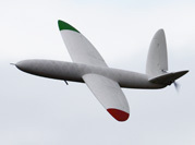
The SULSA began life in something like an inkjet and wound up in the air. (Credit: University of Southhampton)
The SULSA (Southampton University Laser Sintered Aircraft) is an unmanned air vehicle that emerged, layer by layer, from a nylon laser sintering machine that can fabricate plastic or metal objects. In the case of the SULSA, the wings, access hatches, and the rest of the structure of the plane were all printed.
As if that weren't awesome enough, the entire thing snaps together in minutes, no tools or fasteners required. The electric plane has a wingspan of just under 7 feet and a top speed of 100 mph.
Jim Scanlon, one of the project leads at the University of Southhampton, explains in a statement that the technology allows for products to go from conception to reality much quicker and more cheaply.
"The flexibility of the laser-sintering process allows the design team to revisit historical techniques and ideas that would have been prohibitively expensive using conventional manufacturing," Scanlon says. "One of these ideas involves the use of a Geodetic structure... This form of structure is very stiff and lightweight, but very complex. If it was manufactured conventionally it would require a large number of individually tailored parts that would have to be bonded or fastened at great expense."
So apparently when it comes to 3D printing, the sky is no longer the limit. Let's just make sure someone double-checks the toner levels before we start printing the next international space station.
-----
Personal comments:
Industrial production tools back to people?
Fab@Home project
Thursday, July 28. 2011
Decoding DNA With Semiconductors
Via New York Times
By Christopher Capozziello
-----
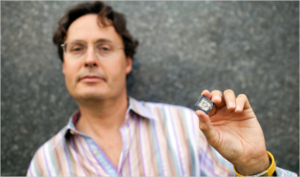
The inventor Jonathan Rothberg with a semiconductor chip used in the Ion Torrent machine.
The inventor of a new machine that decodes DNA with semiconductors has used it to sequence the genome of Gordon Moore, co-founder of Intel, a leading chip maker.
The inventor, Jonathan Rothberg of Ion Torrent Systems in Guilford, Conn., is one of several pursuing the goal of a $1,000 human genome, which he said he could reach by 2013 because his machine is rapidly being improved.
“Gordon Moore worked out all the tricks that gave us modern semiconductors, so he should be the first person to be sequenced on a semiconductor,” Dr. Rothberg said.
At $49,000, the new DNA decoding device is cheaper than its several rivals. Its promise rests on the potential of its novel technology to be improved faster than those of machines based on existing techniques.
Manufacturers are racing to bring DNA sequencing costs down to the point where a human genome can be decoded for $1,000, the sum at which enthusiasts say genome sequencing could become a routine part of medical practice.
But the sequencing of Dr. Moore’s genome also emphasizes how far technology has run ahead of the ability to interpret the information it generates.
Dr. Moore’s genome has a genetic variant that denotes a “56 percent chance of brown eyes,” one that indicates a “typical amount of freckling” and another that confers “moderately higher odds of smelling asparagus in one’s urine,” Dr. Rothberg and his colleagues reported Wednesday in the journal Nature. There are also two genetic variants in Dr. Moore’s genome said to be associated with “increased risk of mental retardation” — a risk evidently never realized. The clinical value of this genomic information would seem to be close to nil.
Dr. Rothberg said he agreed that few genes right now yield useful genetic information and that it will be a 10- to 15-year quest to really understand the human genome. For the moment his machine is specialized for analyzing much smaller amounts of information, like the handful of genes highly active in cancer.
The Ion Torrent machine requires only two hours to sequence DNA, although sample preparation takes longer. The first two genomes of the deadly E. coli bacteria that swept Europe in the spring were decoded on the company’s machines.
The earliest DNA sequencing method depended on radioactivity to mark the four different units that make up genetic material, but as the system was mechanized, engineers switched to fluorescent chemicals. The new device is the first commercial system to decode DNA directly on a semiconductor chip and to work by detecting a voltage change, rather than light.
About 1.2 million miniature wells are etched into the surface of the chip and filled with beads holding the DNA strands to be sequenced. A detector in the floor of the well senses the acidity of the solution in each well, which rises each time a new unit is added to the DNA strands on the bead. The cycle is repeated every few seconds until each unit in the DNA strand has been identified.
Several years ago, Dr. Rothberg invented another DNA sequencing machine, called the 454, which was used to sequence the genome of James Watson, the co-discoverer of the structure of DNA. Dr. Rothberg said he was describing how the machine had “read” Dr. Watson’s DNA to his young son Noah, who asked why he did not invent a machine to read minds.
Dr. Rothberg said he began his research with the idea of making a semiconductor chip that could detect an electrical signal moving across a slice of neural tissue. He then realized the device he had developed was more suited to sequencing DNA.
George Church, a genome technologist at the Harvard Medical School, said he estimated the cost to sequence Dr. Moore’s genome at $2 million. This is an improvement on the $5.7 million it cost in 2008 to sequence Dr. Watson’s genome on the 454 machine, but not nearly as good as the $3,700 spent by Complete Genomics to sequence Dr. Church’s genome and others in 2009.
Dr. Rothberg said he had already reduced the price of his chips to $99 from $250, and today could sequence Dr. Moore’s genome for around $200,000. Because of Moore’s Law — that the number of transistors placeable on a chip doubles about every two years — further reductions in the cost of the DNA sequencing chip are inevitable, Dr. Rothberg said.
Stephan Schuster, a genome biologist at Penn State, said his two Ion Torrent machines were “outstanding,” and enabled a project that would usually have taken two months to be completed in five days.
There is now “a race to the death as to who can sequence faster and cheaper, always with the goal of human resequencing in mind,” Dr. Schuster said.
Monday, July 18. 2011
Chrome OS: The Cloud-Only Problem is Coming Home to Roost
Via OStatic
-----
 Now
that Chromebooks--portable computers based on Google's Chrome OS--are
out in the wild and hands-on reviews are appearing about them, it's
easier to gauge the prospects for this new breed of operating system.
As Jon Buys discussed here on OStatic,
these portables are not without their strong points. However, there
are criticisms appearing about the devices, and the criticisms echo
ones that we made early on. In short, Chromebooks force a cloud-only
compute model that leaves people used to working with local files and
data in the cold.
Now
that Chromebooks--portable computers based on Google's Chrome OS--are
out in the wild and hands-on reviews are appearing about them, it's
easier to gauge the prospects for this new breed of operating system.
As Jon Buys discussed here on OStatic,
these portables are not without their strong points. However, there
are criticisms appearing about the devices, and the criticisms echo
ones that we made early on. In short, Chromebooks force a cloud-only
compute model that leaves people used to working with local files and
data in the cold.
In his OStatic post on Chromebooks, Jon Buys noted that the devices are "built to be the fastest way to get to the web." Indeed, Chromebooks boot in seconds--partly thanks to a Linux core--and deposit the user into an environment that looks and works like the Chrome browser.
However, Cade Metz, writing for The Register, notes this in a review of the Samsung Chromebook, which is available for under $500:
"Running Google's Chrome OS operating system, Chromebooks seek to move everything you do onto the interwebs. Chrome OS is essentially a modified Linux kernel that runs only one native application: Google's Chrome browser….This also means that most of your data sits on the web, inside services like Google Docs…The rub is that the world isn't quite ready for a machine that doesn't give you access to local files."
That's exactly what I felt woud be the shortcoming of devices based on Chrome OS, as seen in this post:
"With Chrome OS, Google is betting heavily on the idea that consumers and business users will have no problem storing data and using applications in the cloud, without working on the locally stored data/applications model that they're used to. Here at OStatic, we always questioned the aggressively cloud-centric stance that Chrome OS is designed to take. Don't users want local applications too? Why don't I just run Ubuntu and have my optimized mix of cloud and local apps? After all, the team at Canonical, which has a few years more experience than Google does in the operating system business, helped create Chrome OS. "
The interesting thing is, though, that Google may have an opportunity to easily address this perceived shortcoming. For example, Chrome OS now has a file manager, and it's not much of a leap to get from a file manager to a reasonable set of ways to store local data and manage it. Odds are that Google will change the way Chrome OS works going forward, making it less cloud-centric. That would seem to be a practical course of action.
Thursday, July 14. 2011
Faster and stronger: next-generation memory tech outperforms flash
Via ars technica
-----

Flash memory is the dominant nonvolatile (retaining information when unpowered) memory thanks to its appearance in solid-state drives (SSDs) and USB flash drives. Despite its popularity, it has issues when feature sizes are scaled down to 30nm and below. In addition, flash has a finite number of write-erase cycles and slow write speeds (on the order of ms). Because of these shortcomings, researchers have been searching for a successor even as consumers snap up flash-based SSDs.
There are currently a variety of alternative technologies competing to replace silicon-based flash memory, such as phase-change RAM (PRAM), ferroelectric RAM (FERAM), magnetoresistive RAM (MRAM), and resistance-change RAM (RRAM). So far, though, these approaches fail to scale down to current process technologies well—either the switching mechanism or switching current perform poorly at the nanoscale. All of them, at least in their current state of development, also lack some commercially-important properties such as write-cycle endurance, long-term data retention, and fast switching speed. Fixing these issues will be a basic requirement for next-gen non-volatile memory.
Or, as an alternative, we might end up replacing this tech entirely. Researchers from Samsung and Sejong University in Korea have published a paper in Nature Materials that describes tanatalum oxide-based (TaOx) resistance-RAM (RRAM), which shows large improvements over current technology in nearly every respect.
RRAM devices work by applying a large enough voltage to switch material that normally acts as an insulator (high-resistance state) into a low-resistance state. In this case, the device is a sandwich structure with a TaO2-x base layer and a thinner Ta2O5-x insulating layer, surrounded by platinum (Pt) electrodes. This configuration, known as metal-insulator-base-metal (MIMB), starts as an insulator, but it can be switched to a low resistance, metal-metal (filament)-base-metal (MMBM) state.
The nature of the switching process is not well understood in this case, but the authors describe it as relying on the creation of conducting filaments that extend through the Ta2O5-x layer. These paths are created by applying sufficiently large voltages, which drive the movement of oxygen ions through a redox (reduction-oxidaton) process.
When in the MIMB state, the interface between the Pt electrode and the Ta2O5-x forms a metal-semiconductor junction known as a Schottky barrier, while the MMBM state forms an ohmic contact. The main difference between these two is that the current-voltage profile is linear and symmetric for ohmic but nonlinear and asymmetric for Schottky. The presence of Schottky barriers is a benefit, as it prevents stray current leakage through an array of multiple devices (important for high-density storage).
The results presented by the authors appear to blow other memory technologies out of the water, in pretty much every way we care about. The devices presented here are 30nm thick, and the switching current is 50 ?A—an order of magnitude smaller than that of PRAM. They also demonstrated an endurance of greater than 1012 switching cycles (higher than the previous best of 1010 and six orders of magnitude higher than that of flash memory at 104-106). The device has a switching time of 10ns, and a data retention time that's estimated to be 10 years operating at 85°C. This type of RRAM also appears to work without problems in a vacuum, unlike previously-demonstrated devices.
This may all seem too good to be true—it should be emphasized that this was only a laboratory-scale demonstration, with 64 devices in an array (therefore capable of storing only 64 bits). There will still be a few years of development needed before we see gigabyte-size drives based on this RRAM memory.
Like all semiconductor device fabrication, advances will be needed to improve nanoscale lithography techniques for large-scale manufacturing and, in this particular case, a better understanding of the basic switching mechanism is also needed. However, based on the results shown here, this new memory technology shows promise for use as a universal memory storage: the same type could be used for storage and working memory.
Monday, July 11. 2011
Toolbox Review: iMSO-104 Oscilloscope for iPad & iPhone
Via makezine
-----

Included tangibles are as follows:
- iMSO-104 Mixed Signal Oscilloscope Hardware
- 1x/10 Analog Probe
- Logic Harness (4 Digital + 1 Ground)
- SMD Grabbers (4 Digital + 1 Ground)
- Screwdriver for Analog Waveform Compensation Adjustment
- Analog tip covers (2 pieces)
The core hardware, based on the Cypress PSoC 3 chip, is housed in a slim enclosure with requisite Apple dock connector, SMB jack for the analog probe, and 5-pin male header to accommodate 4 digital channels + ground. The included set of probes appear well-built, and I estimate they’d withstand the level abuse my other test equipment is subject to. The unit also includes a small blue LED power indicator which turns off whenever the device’s related software becomes inactive.
Software

The iMSO’s software portion is available for free as a Universal app and includes an interactive demo mode to give you an idea of how the unit handles analog signals. The app implements standard digital scope functionality (zoom, trigger, cursor/measurement) with thankfully little UI clutter. In addition to standard menu controls, users can employ familiar pinch-to-zoom gestures as well as control voltage trigger level via onscreen sliders, and double-tap to toggle display infos.
Usage

Right off the bat, I was intrigued at the thought of using the iPad’s 9.7? display and touch input for highly portable ‘scoping. And yes, viewing a sinewave in such a manner does feel satisfyingly slick and moreover, imbues Apple’s hardware with an air of technical sophistication rarely achieved while editing a Pages document or playing Angry Birds. The iMSO software was easily controllable via my iPhone, but I really can’t imagine using it much on that platform when given the option of a much larger display.
While it won’t replace my big ol’ 50MHz CRT benchtop dinosaur, the iMSO’s comparatively humble 5MHz analog bandwidth works well for inspecting audio signals (which I do quite often). Additionally, max voltage limits on the devices inputs (±40V analog 10x, -0.5V/+13V digital) mean I’m likely to reserve use exclusively for low-power audio work. On the digital side, the unit did prove capable when I attempted peeking in on some serial communications between an Arduino board and MCP4921 DAC chip.
The fact that iOS devices use a single port for both power & data, means you’ll have to rely on battery power while using the iMSO. Thankfully, the device + software went easy on my iPad 2?s battery – so power is likely only a concern for those who plan on marathon testing/debugging sessions.
The ~$300 pricetag and bandwidth limitations will likely limit the iMSO’s initial audience – but if those points don’t pose a problem for you, well, this thing is pretty dang sweet. As the IMSO-104 is the first in its category, It will be interesting to see what future developments hold for iOS test equipment – see, we shall.
Thursday, July 07. 2011
Ambient electromagnetic energy harnessed for small electronic devices
Via Physorg
-----
Researchers have discovered a way to capture and harness energy transmitted by such sources as radio and television transmitters, cell phone networks and satellite communications systems. By scavenging this ambient energy from the air around us, the technique could provide a new way to power networks of wireless sensors, microprocessors and communications chips.
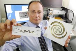
Georgia Tech School of Electrical and Computer Engineering professor Manos Tentzeris holds a sensor (left) and an ultra-broadband spiral antenna for wearable energy-scavenging applications. Both were printed on paper using inkjet technology.
"There is a large amount of electromagnetic energy all around us, but nobody has been able to tap into it," said Manos Tentzeris, a professor in the Georgia Tech School of Electrical and Computer Engineering who is leading the research. "We are using an ultra-wideband antenna that lets us exploit a variety of signals in different frequency ranges, giving us greatly increased power-gathering capability."
A presentation on this energy-scavenging technology was scheduled for delivery July 6 at the IEEE Antennas and Propagation Symposium in Spokane, Wash. The discovery is based on research supported by multiple sponsors, including the National Science Foundation, the Federal Highway Administration and Japan's New Energy and Industrial Technology Development Organization (NEDO).
Communications devices transmit energy in many different frequency ranges, or bands. The team's scavenging devices can capture this energy, convert it from AC to DC, and then store it in capacitors and batteries. The scavenging technology can take advantage presently of frequencies from FM radio to radar, a range spanning 100 megahertz (MHz) to 15 gigahertz (GHz) or higher.
Georgia Tech School of Electrical and Computer Engineering professor Manos Tentzeris displays an inkjet-printed rectifying antenna used to convert microwave energy to DC power. It was printed on flexible material. (Georgia Tech Photo: Gary Meek).
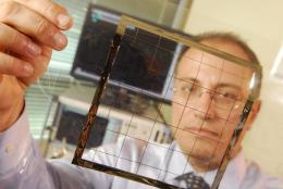
Georgia Tech School of Electrical and Computer Engineering professor Manos Tentzeris displays an inkjet-printed rectifying antenna used to convert microwave energy to DC power. It was printed on flexible material. (Georgia Tech Photo: Gary Meek).
Utilizing ambient electromagnetic energy could also provide a form of system backup. If a battery or a solar-collector/battery package failed completely, scavenged energy could allow the system to transmit a wireless distress signal while also potentially maintaining critical functionalities.
When Tentzeris and his research group began inkjet printing of antennas in 2006, the paper-based circuits only functioned at frequencies of 100 or 200 MHz, recalled Rushi Vyas, a graduate student who is working with Tentzeris and graduate student Vasileios Lakafosis on several projects.
"We can now print circuits that are capable of functioning at up to 15 GHz -- 60 GHz if we print on a polymer," Vyas said. "So we have seen a frequency operation improvement of two orders of magnitude."
The researchers believe that self-powered, wireless paper-based sensors will soon be widely available at very low cost. The resulting proliferation of autonomous, inexpensive sensors could be used for applications that include:
Wednesday, July 06. 2011
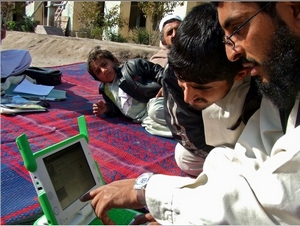
Afghan City Builds DIY Internet Out Of Trash
Via Insteading
-----
Is there such a thing as DIY internet? An amazing open-source project in Afghanistan proves you don’t need millions to get connected.
While visiting family last week, the topic of conversation turned to the internet, net neutrality, and both corporate and government attempts to police the online world. A family member remarked that if they wanted to, the U.S. government could simply turn off the internet and the entire world would be screwed.
Having read this inspiring article by Douglas Rushkoff on Shareable.net, I surprised the room by disagreeing. I said that we didn’t need the corporate built internet, and that if we had to, the people could build their own. Of course, not being that technically minded, I couldn’t offer a concrete idea of how this could be achieved. Until now.
A recent Fast Company article shines a spotlight on the Afghan city of Jalalabad which has a high-speed Internet network whose main components are built out of trash found locally. Aid workers, mostly from the United States, are using the provincial city in Afghanistan’s far east as a pilot site for a project called FabFi.
FabFi is an open-source, FabLab-grown system using common building materials and off-the-shelf electronics to transmit wireless ethernet signals across distances of up to several miles. With Fabfi, communities can build their own wireless networks to gain high-speed internet connectivity—thus enabling them to access online educational, medical, and other resources.
Residents who desire an internet connection can build a FabFi node out of approximately $60 worth of everyday items such as boards, wires, plastic tubs, and cans that will serve a whole community at once.
Jalalabad’s longest link is currently 2.41 miles, between the FabLab and the water tower at the public hospital in Jalalabad, transmitting with a real throughput of 11.5Mbps (compared to 22Mbps ideal-case for a standards compliant off-the-shelf 802.11g router transitting at a distance of only a few feet). The system works consistently through heavy rain, smog and a couple of good sized trees.
With millions of people still living without access to high-speed internet, including much of rural America, an open-source concept like FabFi could have profound ramifications on education and political progress.
Because FabFi is fundamentally a technological and sociological research endeavor, it is constantly growing and changing. Over the coming months expect to see infrastructure improvements to improve stability and decrease cost, and added features such as meshing and bandwidth aggregation to support a growing user base.
In addition to network improvements, there are plans to leverage the provided connectivity to build online communities and locally hosted resources for users in addition to MIT OpenCourseWare, making the system much more valuable than the sum of its uplink bandwidth. Follow the developments on the FabFi Blog.
Quicksearch
Popular Entries
- The great Ars Android interface shootout (131506)
- Norton cyber crime study offers striking revenue loss statistics (102392)
- MeCam $49 flying camera concept follows you around, streams video to your phone (100517)
- The PC inside your phone: A guide to the system-on-a-chip (58691)
- Norton cyber crime study offers striking revenue loss statistics (58621)
Categories

Show tagged entries
Syndicate This Blog
Calendar
|
|
July '26 | |||||
| Mon | Tue | Wed | Thu | Fri | Sat | Sun |
| 1 | 2 | 3 | 4 | 5 | ||
| 6 | 7 | 8 | 9 | 10 | 11 | 12 |
| 13 | 14 | 15 | 16 | 17 | 18 | 19 |
| 20 | 21 | 22 | 23 | 24 | 25 | 26 |
| 27 | 28 | 29 | 30 | 31 | ||