Tuesday, February 19. 2013
3Doodler 3D printer pen hits Kickstarter
Via Slashgear
-----
3D printers are undeniably cool, but their price also puts them out of the reach of most; that’s where 3Doodler steps in, a 3D printing pen hitting Kickstarter today and promising to make sketches physical. The chubby stylus squirts out of a stream of thermoplastic from its 270 degree-C nib, which is instantly cooled by an integrated fan. By laying different streams of plastic, tugging up streams of it to make 3D structures, and piecing different layers together, you can create 3D designs on a budget.

In fact, early Kickstarter backers will be able to get the 3Doodler from $50, though that award tier is already nearly halfway claimed at time of writing. Next is the $75 bracket, which should stick around a little longer, with the eventual Kickstarter goal being $30,000.
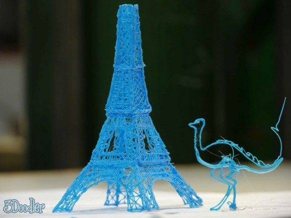
Unlike traditional printers, which require programming, the 3Doodler takes a more abstract approach. You can freeform draw sketches, or alternatively trace out patterns that have been printed, and then peel the set plastic off; 3Doodler suggests possibilities include jewelry, 3D models, artwork, and more.
It’s not going to be the way you print your next coffee cup or car wheel, as we’ve seen promised from regular 3D printers, but the plug-and-play approach has plenty of appeal nonetheless. The Kickstarter runs for the next month, with first deliveries expected in the fall of 2013 assuming it’s funded.
Thursday, February 14. 2013
The future of mobile CPUs, part 1: Today’s fork in the road
Via ars technica
-----
Mobile computing's rise from niche market to the mainstream is among the most significant technological trends in our lifetimes. And to a large extent, it's been driven by the bounty of Moore’s Law—the rule that transistor density doubles every 24 months. Initially, most mobile devices relied on highly specialized hardware to meet stringent power and size budgets. But with so many transistors available, devices inevitably grew general-purpose capabilities. Most likely, that wasn't even the real motivation. The initial desire was probably to reduce costs by creating a more flexible software ecosystem with better re-use and faster time to market. As such, the first smartphones were very much a novelty, and it took many years before the world realized the potential of such devices. Apple played a major role by creating innovative smartphones that consumers craved and quickly adopted.
To some extent, this is where we still stand today. Smartphones are still (relatively) expensive and primarily interesting to the developed world. But over the next 10 years, this too will change. As Moore’s Law rolls on, the cost of a low-end smartphone will decline. At some point, the incremental cost will be quite minimal and many feature phones of today will be supplanted by smartphones. A $650 unsubsidized phone is well beyond the reach of most of the world compared to a $20 feature phone, but a $30 to $40 smartphone would naturally be very popular.
In this grand progression, 2013 will certainly be a significant milestone for mobile devices, smartphones and beyond. It's likely to be the first year in which tablets out-ship notebooks in the US. And in the coming years, this will lead to a confluence of high-end tablets and ultra-mobile notebooks as the world figures out how these devices co-exist, blend, hybridize, and/or merge.
Against this backdrop, in this two-part series, we'll explore the major trends and evolution for mobile SoCs. More importantly, we'll look to where the major vendors are likely going in the next several years.
Tablet and phone divergence
While phones and tablets are mobile devices that often share a great deal of software, it's becoming increasingly clear the two are very different products. These two markets have started to diverge and will continue doing so over time.
From a technical perspective, smartphones are far more compact and power constrained. Smartphone SoCs are limited to around 1W, both by batteries and by thermal dissipation. The raison d’etre of a smartphone is connectivity, so a cellular modem is an absolute necessity. For the cost sensitive-models that make up the vast majority of the market, the modem is integrated into the SoC itself. High-end designs favor discrete modems with a greater power budget instead. The main smartphone OSes today are iOS and Android, though Windows is beginning to make an appearance (perhaps with Linux or BlackBerry on the horizon). Just as importantly, phone vendors like HTC must pass government certification and win the approval of carriers. There is very much a walled-garden aspect, where carriers control which devices can be attached to their networks, and in some cases devices can only be sold through a certain carrier. The business model places consumers quite far removed from the actual hardware.
In contrast, tablets are far more akin to the PC both technically and economically. The power budget for tablet SoCs is much greater, up to 4W for a passively cooled device and as high as 7-8W for systems with fans. This alone means there is a much wider range of tablet designs than smartphones. Moreover, the default connectivity for tablets is Wi-Fi rather than a cellular modem. The vast majority of tablets do not have cellular modems, and even fewer customers actually purchase a wireless data plan. As a result, cellular modems are almost always optional discrete components of the platform. The software ecosystem is relatively similar, with Microsoft, Apple, and Google OSes available. Because tablets eschew cellular modems, the time to market is faster, and they are much more commonly sold directly to consumers rather than through carriers. In terms of usage models, tablets are much more PC-like, with reasonable-sized screens that make games and media more attractive.
Looking forward, these distinctions will likely become more pronounced. Many tablets today use high-end smartphone SoCs, but the difference in power targets and expected performance is quite large. As the markets grow in volume, SoCs will inevitably bifurcate to focus on one market or the other. Even today, Apple is doing so, with the A6 for phones and the larger A6X for tablets. Other vendors may need to wait a few years to have the requisite volume, but eventually the two markets will be clearly separate.
Horizontal business model evolution
Another aspect of the mobile device market that is currently in flux and likely to change in the coming years is the business model for the chip and system vendors. Currently, Apple is the only company truly pursuing a vertically integrated model, where all phones and tablets are based on Apple’s own SoC designs and iOS. The tight integration between hardware and software has been a huge boon for Apple, and it has yielded superb products.
The rest of the major SoC vendors (e.g., Intel, Qualcomm, Nvidia, TI, Mediatek, etc.) have stayed pretty far away from actual mobile devices. These companies tend to focus on horizontal business models that avoid competing with customers or suppliers.
In the long term, mobile devices are likely to evolve similarly to the PC and favor a horizontal business model. The real advantage is one of flexibility; as costs drop and the market expands, it will be increasingly necessary for vendors like HTC to offer a wide range of phones based on radically different SoCs. While a vertically integrated company like Apple can focus and maintain leadership in a specific (and highly lucrative) niche, it would be very difficult to expand in many growing areas of the market. The differences between an iPhone 6 and a $20 feature phone are tremendous and would be very difficult for a single company to bridge.
However, SoC vendors will attempt to reap the benefits of vertical integration by providing complete reference platforms to OEMs. Conceptually, this is a form of "optional" system integration, where the phone vendor or carrier can get the entire platform from the SoC supplier. This has the principal advantages of reducing time to market while also providing a baseline quality and experience for consumers. Currently, this approach has mostly been tested in emerging markets, but it's likely to become more common over time. There is a crucial distinction between reference platforms and vertical integration. Namely, OEMs can always choose to customize a platform to differentiate, and the SoC vendor avoids dealing with consumers directly. Typically, most of the customization is in terms of software on top of a base operating system.
Focus on the intellectual
One unique aspect of mobile devices is the availability and prevalence of third-party intellectual property (IP). Unlike the PC industry, it is a common practice for SoC vendors to use a variety of external and internal IP. ARM and Imagination Technologies are the best known IP vendors, with reputations established for CPUs and GPUs respectively. Most major SoC blocks are available as IP, which creates a very broad and diverse ecosystem. Even vertically integrated companies such as Apple rely on third-party IP.
Vertical integration of IP within the context of a single chip makes tremendous sense and is likely to be the future for most SoC vendors. While third-party IP is highly flexible and can reduce time to market and development costs, it comes with real trade-offs. The licensing costs are typically on a per-unit basis and thus are increasingly problematic at high volume. At a certain point, the variable licensing costs outweigh the fixed development costs, and it makes more sense to use internal resources.
Moreover, there are risks associated with third-party IP that are more difficult to control. For instance, Intel’s Clovertrail tablet has been delayed, likely due to problems with the Imagination Technologies graphics drivers for Windows 8. And third-party IP is often intended to address a wider market and may not fit with the intentions of a specific vendor. For instance, licensed ARM cores cannot be substantially modified, which removes an element of flexibility for companies with good CPU design teams.
Over the next decade, the higher volume vendors will likely focus on reducing the amount of external IP and emphasizing internal development expertise. That means licensing ARM’s instruction set and designing custom cores (as Apple has done with the A6), rather than using the stock cores. In other cases, SoC vendors will develop or acquire the necessary building blocks, such as baseband processors. One area where third-party IP will probably continue to be popular is graphics, largely because of the complexity of the software stack. Modern graphics APIs and drivers are very challenging, and the development cost may prove prohibitive for all but the very largest companies.
Manufacturing trends
The SoCs for mobile devices are inextricably tied to semiconductor manufacturing, and any look into the future must be based on a realistic assessment of the underlying technology. While Moore’s Law has continued to operate, certain aspects of silicon scaling stopped roughly a decade ago. In particular, shrinking transistors ceased granting an intrinsic increase in performance. The industry adapted and embraced a number of novel technologies to boost performance where appropriate.
Perhaps the biggest question looming over the industry is the fate of Moore’s Law and whether transistors will continue to shrink. Ten years is a very long time to make technical projections with any degree of certainty. However, there is no reason to believe that process technology scaling will stop—the advantages of shrinking are still quite large. In the next few years, the industry will move from 193nm conventional lithography to 13nm EUV lithography, which should last for quite some time. Going forward, though, innovations in materials will be absolutely necessary for Moore’s Law, and these will happen at a faster pace. To date, the major changes in manufacturing have been copper interconnects, strained silicon, high-k/metal gates, and now fully depleted transistors (e.g. FinFETs or FD-SOI), and there is plenty of promising research for the roadmap.
However, these new techniques are increasingly expensive from both a development and variable cost standpoint. Each new technique tends to winnow the field of manufacturers a bit more. Fujitsu and TI both have excellent process technology, but they could not afford to develop high-k/metal gates at the 32nm node and instead moved to a fabless model for digital logic. It's nearly certain that the number of leading edge manufacturers will shrink to just a handful. Intel, TSMC, and Samsung have the volume and can continue to afford the pace of Moore’s Law, but the economics may be prohibitive for everyone else.
Even so, a fabless model is not necessarily a panacea because of the rising variable costs. In the past, TSMC and many foundries have been able to avoid expensive techniques, but that option is no longer feasible. For instance, conventional lithography cannot draw features below 80nm without multiple patterning. If double patterning is required for a process step, it will cut the throughput of that step in half. FinFETs are similarly complex and will impact throughput as well. These costs (along with profits for TSMC or GlobalFoundries) are ultimately passed along to foundry customers as higher wafer prices.
Long-term, this translates into an advantage for the two IDMs: Intel and Samsung. First, an IDM essentially pockets the profits from both manufacturing and design, whereas fabless companies only collect the latter and must give up the former to TSMC or GlobalFoundries. Second, IDMs have greater control over the supply chain and are less likely to be subject to availability problems as a result of manufacturing challenges. Third, the cost delta between IDMs and foundries is likely to erode for the technical reasons outlined above.
One new technique which will be adopted across the industry over the next decade is 3D integration. Many mobile devices already use chip stacking, where several different integrated circuits are vertically stacked in a single package. Typically, chip stacking relies on connecting different layers of the stack with low-density bond wires or solder bumps. However, many companies are actively working on solutions to connect different layers via through-silicon vias (TSVs), which are much denser and offer greater connectivity and power savings. 3D integration using TSVs is far more sophisticated than 3D packaging, since a single integrated circuit can span multiple layers. The primary use case for 3D integration is packaging high-speed memory with an SoC to deliver superior bandwidth for graphics. Currently, the only products using 3D integration are FPGAs from Xilinx, but the technology should become relatively common during the next few years, and it should be available later to all mobile vendors.
Manufacturing roadmap
Currently, Intel is about two years ahead of the rest of the industry in terms of high-volume manufacturing for high-performance products (i.e. server, desktop, and notebook SoCs). Intel’s 22nm Ivy Bridge went into production at the end of 2011, around the same time that TSMC started producing 28nm GPUs. Additionally, Intel tends to be about one node ahead of the industry for performance features such as strained silicon, high-k/metal gates, and FinFETs (e.g. Intel introduced high-k/metal gates in 2007, foundries in 2011 and 2012). Looking forward, Intel’s manufacturing is expected to stay on a two-year cadence at least through the 10nm node in late 2015, and there is no reason to expect any deviation from this trend further out.
However, Intel’s mobile SoC designs are two years behind the cutting edge of manufacturing, with 32nm SoCs shipping today. Over the next two to three years, Intel will pick up the pace of SoC development, hitting 22nm by the end of 2013 and 14nm by the end of 2014. Long-term, the mobile SoCs will probably reach about six months behind the PC designs in terms of manufacturing, driven by cost constraints. Specifically, Intel’s fabs are quite expensive for the first year, when yields are still ramping up and the factory is depreciating. The ASPs for notebooks and desktops are high enough to amortize these costs. After six to 12 months, the costs are much lower and more amenable to phone and tablet products.
Looking at the foundries is a little more challenging and confusing. First of all, TSMC, GlobalFoundries, and Samsung tend to announce production well in advance of actual mobile SoCs shipping. However, assuming a two-year cadence is a very reasonable guideline. That places the 20nm planar node (and attendant SoCs) in late 2013 or early 2014.
The 14nm node will be quite problematic for the foundries, though. Without EUV, it will be necessary to use double patterning on the metal interconnects, which will substantially increase costs. Instead, the foundries are developing a hybrid process that uses a 14nm FinFET to boost performance, but they're keeping the same 20nm metal interconnect. From a practical standpoint, this means the foundry 14nm process will be comparable to Intel’s 22nm process in terms of performance and density, despite the name. The foundries claim that the hybrid 14nm/20nm process will arrive in 2015, which seems somewhat optimistic given the challenges involved in achieving yield for FinFETs. Moreover, that will make the transition to a 10nm node even more difficult, as the foundries will have to move from 20nm interconnects to 10nm interconnects and skip a generation.
Long-term, it seems like the foundries are expending significant effort to narrow the gap with Intel. Historically, this has proven to be an elusive goal, and there are few fundamental changes that suggest this would be feasible. It's most likely Intel’s mobile SoCs will accelerate over the next few years and ultimately reach and then maintain a 12 to 18 month lead in process technology (and hence density) over the competition. The real question is how fast the foundries will be able to implement techniques like FinFETs and other performance enhancements. It is quite possible this gap could narrow from the current four to five years down to three to four years.
In the conclusion of this series, we will explore how these trends come together and impact the leading mobile SoC vendors and where they are expected to evolve over the next five to ten years.
David Kanter is Principal Analyst and Editor-in-Chief at Real World Tech,
which focuses on microprocessors, servers, graphics, computers, and
semiconductors. He is also a consultant specializing in intellectual
property evaluation/development and technical/competitive analysis.
Monday, February 11. 2013
Researchers create robot exoskeleton that is controlled by a moth running on a trackball
Via ExtremTech
-----

If you’re terrified of the possibility that humanity will be dismembered by an insectoid master race, equipped with robotic exoskeletons (or would that be exo-exoskeletons?), look away now. Researchers at the University of Tokyo have strapped a moth into a robotic exoskeleton, with the moth successfully controlling the robot to reach a specific location inside a wind tunnel.
In all, fourteen male silkmoths were tested, and they all showed a scary aptitude for steering a robot. In the tests, the moths had to guide the robot towards a source of female sex pheromone. The researchers even introduced a turning bias — where one of the robot’s motors is stronger than the other, causing it to veer to one side — and yet the moths still reached the target.
As you can see in the photo above, the actual moth-robot setup is one of the most disturbing and/or awesome things you’ll ever see. In essence, the polystyrene (styrofoam) ball acts like a trackball mouse. As the silkmoth walks towards the female pheromone, the ball rolls around. Sensors detect these movements and fire off signals to the robot’s drive motors. At this point you should watch the video below — and also not think too much about what happens to the moth when it’s time to remove the glued-on stick from its back.
Fortunately, the Japanese researchers aren’t actually trying to construct a moth master race: In reality, it’s all about the moth’s antennae and sensory-motor system. The researchers are trying to improve the performance of autonomous robots that are tasked with tracking the source of chemical leaks and spills. “Most chemical sensors, such as semiconductor sensors, have a slow recovery time and are not able to detect the temporal dynamics of odours as insects do,” says Noriyasu Ando, the lead author of the research. “Our results will be an important indication for the selection of sensors and models when we apply the insect sensory-motor system to artificial systems.”

Of course, another possibility is that we simply keep the moths. After all, why should we spend time and money on an artificial system when mother nature, as always, has already done the hard work for us? In much the same way that miners used canaries and border police use sniffer dogs, why shouldn’t robots be controlled by insects? The silkmoth is graced with perhaps the most sensitive olfactory system in the world. For now it might only be sensitive to not-so-useful scents like the female sex pheromone, but who’s to say that genetic engineering won’t allow for silkmoths that can sniff out bombs or drugs or chemical spills?
Who nose: Maybe genetically modified insects with robotic exoskeletons are merely an intermediary step towards real nanobots that fly around, fixing, cleaning, and constructing our environment.
Tuesday, January 29. 2013
The End of an Era: Intel's Desktop Motherboard Business to Ramp Down Over Next 3 Years
Via AnandTech
-----
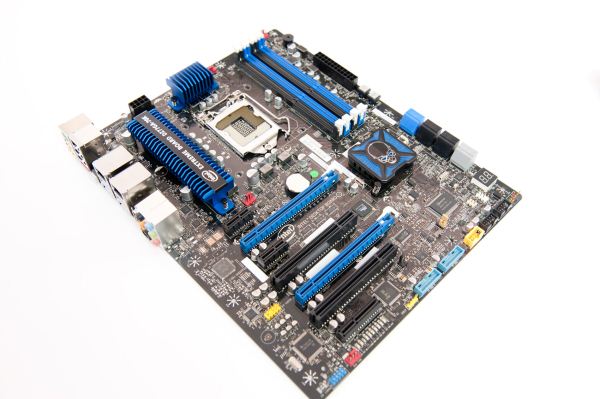
Today Intel made a sobering, but not entirely unexpected announcement: over the next 3 years Intel will be ramping down its own desktop motherboard business. Intel will continue to supply desktop chipsets for use by 3rd party motherboard manufacturers like ASUS, ASRock and Gigabyte, but after 2013 it will no longer produce and sell its own desktop mITX/mATX/ATX designs in the channel. We will see Haswell motherboards from the group, but that will be the last official hurrah. Intel will stop developing desktop motherboards once the Haswell launch is completed. All Intel boards, including upcoming Haswell motherboards, will carry a full warranty and will be supported by Intel during that period.
This isn't a workforce reduction. Most of the folks who worked in Intel's surprisingly small desktop motherboard division will move on to other groups within Intel that can use their talents. Intel's recently announced NUC will have a roadmap going forward, and some of the desktop board folks will move over there. Intel will continue to produce barebones motherboards for its NUC and future versions of the platform.
Intel will also continue to produce its own form factor reference designs (FFRDs) for Ultrabooks and tablets, which will be where many of these employees will end up as well. As of late Intel has grown quite fond of its FFRD programs, allowing it a small taste of vertical integration (and the benefits that go along with it) without completely alienating its partners. This won't be a transfer of talent to work on smartphone FFRDs at this time however.
The group within Intel responsible for building reference designs that are used internally for testing as well as end up as the base for many 3rd party motherboards will not be impacted by this decision either. The reference board group will continue to operate and supply reference designs to Intel partners. This is good news as it means that you shouldn't see a reduction in quality of what's out there.
It's not too tough to understand why Intel would want to wind down its
desktop motherboard business. Intel has two options to keep Wall Street
happy: ship tons of product with huge margins and/or generate additional
profit (at forgiveably lower margins) that's not directly tied to the
PC industry. The overwhelming majority of Intel's business is in the
former group. The desktop motherboards division doesn't exactly fit
within that category. Motherboards aren't good high margin products,
which makes the fact that Intel kept its desktop board business around
this long very impressive. Intel doesn't usually keep drains on margins
around for too long (look how quickly Intel exited the de-emphasized its consumer SSD business).
The desktop motherboard business lasted so long as a way to ensure that Intel CPUs had a good, stable home (you can't sell CPUs if motherboard quality is questionable). While there was a need for Intel to build motherboards and reference designs 15 years ago, today what comes out of Taiwan is really quite good. Intel's constant integration of components onto the CPU and the resulting consolidation in the motherboard industry has helped ensure that board quality went up.
There's also the obvious motivation: the desktop PC business isn't exactly booming. Late last year word spread of Intel's plans for making Broadwell (14nm Core microprocessor in 2014) BGA-only. While we'll continue to see socketed CPUs beyond that, the cadence will be slower than what we're used to. The focus going forward will be on highly integrated designs, even for the desktop (think all-in-ones, thin mini-ITX, NUC, etc...). Couple that reality with low board margins and exiting the desktop motherboard business all of the sudden doesn't sound like a bad idea for Intel.
In the near term, this is probably good for the remaining Taiwanese
motherboard manufacturers. They lose a very competent competitor,
although not a particularly fierce one. In the long run, it does
highlight the importance of having a business not completely tied to
desktop PC motherboard sales.
Friday, January 25. 2013
Electromagnetic Harvester draws power from the world around you
Via DVICE
-----
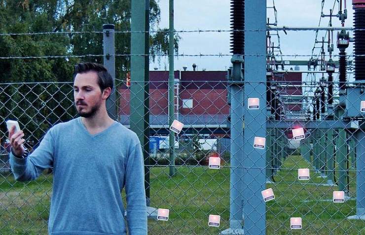
No matter how many times you watch The Matrix, the creepiest part is seeing the whole of humanity hooked up to pods to act as living power generators for their robot masters. Now Germany-based designer Dennis Siegel has created a kind of mini version of this idea that he calls an Electromagnetic Harvester.
The tiny device allows him to draw redundant energy from household appliances, mobile devices, and even outside aerial electrical lines. An LED light indicates when power is effectively being drawn in, and that power is conveniently stored in what appears to be a common AA battery. According to Siegel, it takes the Electromagnetic Harvester about one day to fully charge one of the batteries, depending on the strength of the electromagnetic field being sourced.
You can see video of the Electromagnetic Harvester in action in the video below.
MeCam $49 flying camera concept follows you around, streams video to your phone
Via liliputing
-----
Always Innovating is working on a tiny flying video camera called the MeCam. The camera is designed to follow you around and stream live video to your smartphone, allowing you to upload videos to YouTube, Facebook, or other sites.
And Always Innovating thinks the MeCam could eventually sell for just $49.
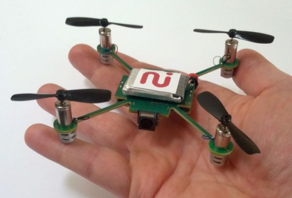
The camera is docked in a nano copter with 4 spinning rotors to keep it aloft. There are 14 different sensors which help the copter detect objects around it so it won’t bump into walls, people. or anything else.
Always Innovating also includes stabilization technology so that videos shouldn’t look too shaky.
Interestingly, there’s no remote control. Instead, you can control the MeCam in one of two ways. You can speak voice commands to tell it, for instance, to move up or down. Or you can enable the “follow-me” feature which tells the camera to just follow you around while shooting paparazzi-style video.
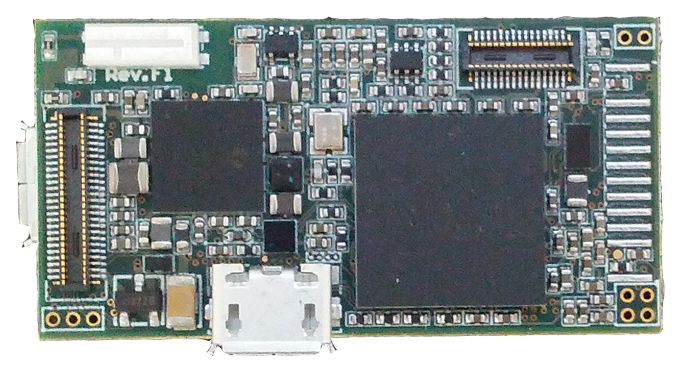
The MeCam features an Always Innovating module with an ARM Cortex-A9 processor, 1GB of RAM, WiFI, and Bluetooth.
The company hopes to license the design so that products based on the MeCam will hit the streets in early 2014.
If Always Innovating sounds familiar, that’s because it’s the same company that brought us the modular Touch Book and Smart Book products a few years ago.
If the MeCam name sounds familiar, on the other hand, it’s probably worth pointing out that the Always Innovating flying camera is not related the wearable camera that failed to come close to meeting its fundraising goals last year.
Tuesday, January 22. 2013
3D printer to carve out world's first full-size building
Via c|net
-----

A rendering of the "Landscape House" by architect Janjaap Ruijssenaars.
(Credit: Universe Architecture)
Sure, we've heard of 3D-printed iPhone cases, dinosaur bones, and even a human fetus -- but something massive, like a building?
This is exactly what architect Janjaap Ruijssenaars has been working on. The Dutch native is planning to build what he calls a "Landscape House." This structure is two-stories and is laid out in a figure-eight shape. The idea is that this form can borrow from nature and also seamlessly fit into the outside world.
Ruijssenaars describes it on his Web site as "one surface folded in an endless mobius band," where "floors transform into ceilings, inside into outside."
The production of the building will be done on a 3D printer called the D-Shape, which was invented by Enrico Dini. The D-Shape uses a stereolithography printing process with sand and a binding agent -- letting builders create structures that are supposedly as strong as concrete.
According to the Los Angeles Times, the printer will lay down thousands of layers of sand to create 20 by 30-foot sections. These blocks will then be used to compile the building.
The "Landscape House" will be the first 3D-printed building and is estimated to cost between $5 million and $6 million, according to the BBC. Ruijssenaars plans to have it done sometime in 2014.
Monday, January 21. 2013
Filabot Makes 3D Printing Cheaper By Recycling Old Plastic
Via WebProNews
-----

Filament is expensive. Ask any 3D printing enthusiast and they will agree that the cost of the plastic filament used to print objects is oftentimes overpriced. If only there was a product that let you recycle all the worthless plastic sitting around your house into usable filament. Oh wait, there totally is.
Say hello to Filabot, a new machine that melts down junk plastic into the plastic filament used by the majority of desktop 3D printers. The machine can process a variety of plastics including HDPE, LDPE, ABS and PLA. The latter two are sold by major 3D printing companies, but now you can make your own if you’re up to melting down a few of your LEGO pieces.
Filabot already had a successful funding run on Kickstarter early last year when the creator, Tyler McNaney, asked for $10,000. In the end, he received $32,330 from 156 backers. Sixty-seven of those backers will be receiving their very own Filabot.
Not only is Filabot a great idea, but it solves one of the major hurdles facing 3D printing – sustainability. Not all 3D printers yet support PLA, a bio-degradable plastic. With Filabot, most plastics can now be melted down into filament to be used in future designs. It saves the creator money while putting the plastic in something besides a landfill. Now that’s what I call a win-win situation.
Tuesday, January 08. 2013
Intel, ARM, tablets and desktop: Where is processing going next?
Tuesday, December 11. 2012
IBM silicon nanophotonics speeds servers with 25Gbps light
Via Slash Gear
-----
IBM has developed a light-based data transfer system delivering more than 25Gbps per channel, opening the door to chip-dense slabs of processing power that could speed up server performance, the internet, and more. The company’s research into silicon integrated nanophotonics addresses concerns that interconnects between increasingly powerful computers, such as mainframe servers, are unable to keep up with the speeds of the computers themselves. Instead of copper or even optical cables, IBM envisages on-chip optical routing, where light blasts data between dense, multi-layer computing hubs.

“This future 3D-integated chip consists of several layers connected with each other with very dense and small pitch interlayer vias. The lower layer is a processor itself with many hundreds of individual cores. Memory layer (or layers) are bonded on top to provide fast access to local caches. On top of the stack is the Photonic layer with many thousands of individual optical devices (modulators, detectors, switches) as well as analogue electrical circuits (amplifiers, drivers, latches, etc.). The key role of a photonic layer is not only to provide point-to-point broad bandwidth optical link between different cores and/or the off-chip traffic, but also to route this traffic with an array of nanophotonic switches. Hence it is named Intra-chip optical network (ICON)” IBM
Optical interconnects are increasingly being used to link different server nodes, but by bringing the individual nodes into a single stack the delays involved in communication could be pared back even further. Off-chip optical communications would also be supported, to link the data-rich hubs together.
Although the photonics system would be considerably faster than existing links – it supports multiplexing, joining multiple 25Gbps+ connections into one cable thanks to light wavelength splitting – IBM says it would also be cheaper thanks to straightforward manufacturing integration:
“By adding a few processing modules into a high-performance 90nm CMOS fabrication line, a variety of silicon nanophotonics components such as wavelength division multiplexers (WDM), modulators, and detectors are integrated side-by-side with a CMOS electrical circuitry. As a result, single-chip optical communications transceivers can be manufactured in a conventional semiconductor foundry, providing significant cost reduction over traditional approaches” IBM
Technologies like the co-developed Thunderbolt from Intel and Apple have promised affordable light-based computing connections, but so far rely on more traditional copper-based links with optical versions further down the line. IBM says its system is “primed for commercial development” though warns it may take a few years before products could actually go on sale.
Quicksearch
Popular Entries
- The great Ars Android interface shootout (131504)
- Norton cyber crime study offers striking revenue loss statistics (102380)
- MeCam $49 flying camera concept follows you around, streams video to your phone (100515)
- The PC inside your phone: A guide to the system-on-a-chip (58690)
- Norton cyber crime study offers striking revenue loss statistics (58609)
Categories

Show tagged entries
Syndicate This Blog
Calendar
|
|
July '26 | |||||
| Mon | Tue | Wed | Thu | Fri | Sat | Sun |
| 1 | 2 | 3 | 4 | 5 | ||
| 6 | 7 | 8 | 9 | 10 | 11 | 12 |
| 13 | 14 | 15 | 16 | 17 | 18 | 19 |
| 20 | 21 | 22 | 23 | 24 | 25 | 26 |
| 27 | 28 | 29 | 30 | 31 | ||