Entries tagged as hardware
Tuesday, January 08. 2013
Intel, ARM, tablets and desktop: Where is processing going next?
Tuesday, December 11. 2012
IBM silicon nanophotonics speeds servers with 25Gbps light
Via Slash Gear
-----
IBM has developed a light-based data transfer system delivering more than 25Gbps per channel, opening the door to chip-dense slabs of processing power that could speed up server performance, the internet, and more. The company’s research into silicon integrated nanophotonics addresses concerns that interconnects between increasingly powerful computers, such as mainframe servers, are unable to keep up with the speeds of the computers themselves. Instead of copper or even optical cables, IBM envisages on-chip optical routing, where light blasts data between dense, multi-layer computing hubs.

“This future 3D-integated chip consists of several layers connected with each other with very dense and small pitch interlayer vias. The lower layer is a processor itself with many hundreds of individual cores. Memory layer (or layers) are bonded on top to provide fast access to local caches. On top of the stack is the Photonic layer with many thousands of individual optical devices (modulators, detectors, switches) as well as analogue electrical circuits (amplifiers, drivers, latches, etc.). The key role of a photonic layer is not only to provide point-to-point broad bandwidth optical link between different cores and/or the off-chip traffic, but also to route this traffic with an array of nanophotonic switches. Hence it is named Intra-chip optical network (ICON)” IBM
Optical interconnects are increasingly being used to link different server nodes, but by bringing the individual nodes into a single stack the delays involved in communication could be pared back even further. Off-chip optical communications would also be supported, to link the data-rich hubs together.
Although the photonics system would be considerably faster than existing links – it supports multiplexing, joining multiple 25Gbps+ connections into one cable thanks to light wavelength splitting – IBM says it would also be cheaper thanks to straightforward manufacturing integration:
“By adding a few processing modules into a high-performance 90nm CMOS fabrication line, a variety of silicon nanophotonics components such as wavelength division multiplexers (WDM), modulators, and detectors are integrated side-by-side with a CMOS electrical circuitry. As a result, single-chip optical communications transceivers can be manufactured in a conventional semiconductor foundry, providing significant cost reduction over traditional approaches” IBM
Technologies like the co-developed Thunderbolt from Intel and Apple have promised affordable light-based computing connections, but so far rely on more traditional copper-based links with optical versions further down the line. IBM says its system is “primed for commercial development” though warns it may take a few years before products could actually go on sale.
Monday, December 03. 2012
Kinect like device: ASUS Xtion

Here is a Kinect-like device from ASUS, which proposed a SDK based on openNI (standard libraries that manage natural interactions issued by different kind of devices). This product can be an interesting alternative to the Microsoft Kinect device for research projects, proposing examples in C++, C# and Java.
Specifications
| Power Consumption | below 2.5W |
| Distance of Use | Between 0.8m and 3.5m |
| Field of View | 58° H, 45° V, 70° D (Horizontal, Vertical, Diagonal) |
| Sensor | RGB& Depth& Microphone*2 |
| Depth Image Size | VGA (640x480) : 30 fps QVGA (320x240): 60 fps |
| Resolution | SXGA (1280*1024) |
| Platform | Intel X86 & AMD |
| OS Support | Win 32/64 : XP , Vista, 7 Linux Ubuntu 10.10: X86,32/64 bit Android(by request) |
| Interface | USB2.0 |
| Software | software development kits(OPEN NI SDK bundled) |
| Programming Language | C++/C# (Windows) C++(Linux) JAVA |
| Operation Environment | Indoor |
| Dimensions | 18 x 3.5 x 5 cm |
Monday, November 26. 2012
Two-tonne Witch computer gets a reboot
Via BBC
-----
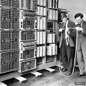
The machine cranked through the boring calculations atomic scientists once had to do
Kevin Murrell who discovered the computer explains how it was brought back to life
The world's oldest original working digital computer is going on display at The National Museum of Computing in Buckinghamshire.
The Witch, as the machine is known, has been restored to clattering and flashing life in a three-year effort.
In its heyday in the 1950s the machine was the workhorse of the UK's atomic energy research programme.
A happy accident led to its discovery in a municipal storeroom where it had languished for 15 years.
Cleaning upThe machine will make its official public debut at a special ceremony at The National Museum of Computing (TNMOC) in Bletchley Park on 20 November. Attending the unveiling will be some of its creators as well as staff that used it and students who cut their programming teeth on the machine.
Design and construction work on the machine began in 1949 and it was built to aid scientists working at the UK's Atomic Energy Research Establishment at Harwell in Oxfordshire. The 2.5 tonne machine was created to ease the burden on scientists by doing electronically the calculations that previously were done using adding machines.
The machine first ran in 1951 and was known as the Harwell Dekatron - so named for the valves it used as a memory store. Although slow - the machine took up to 10 seconds to multiply two numbers - it proved very reliable and often cranked up 80 hours of running time in a week.
By 1957 the machine was being outstripped by faster, smaller computers and it was handed over to the Wolverhampton and Staffordshire Technical College (more recently Wolverhampton University) where it was used to teach programming and began to be called the Witch (Wolverhampton Instrument for Teaching Computation from Harwell).
In 1973 it was donated to Birmingham's Museum of Science and Industry and was on show for 24 years until 1997 when the museum closed and the machine was dismantled and put into storage.
By chance Kevin Murrell, one of the TNMOC's trustees, spotted the control panel of the Witch in a photograph taken by another computer conservationist who had been in the municipal store seeking components for a different machine.
Mr Murrell said that as a "geeky teenager" he had regularly seen the Witch during many trips to the museum and instantly recognised its parts in the background of the photograph.
On subsequent trips to the storage facility the various parts of the Witch were found, retrieved and then taken to the museum at Bletchley where restoration began.
The restoration effort was led by conservationist Delwyn Holroyd who said it was "pretty dirty" when the machine first arrived at Bletchley. Remarkably, he said, it had not suffered too much physical damage and the restoration team has been at pains to replace as little as possible. The vast majority of the parts on the machine, including its 480 relays and 828 Dekatron tubes, are entirely original, he said.
Said Mr Murrell: "It's important for us to have a machine like this back in working order as it gives us an understanding of the state of technology in the late 1940s in Britain."
Wednesday, November 21. 2012
3D printing vending machine automates the invention process
Via DVICE
-----
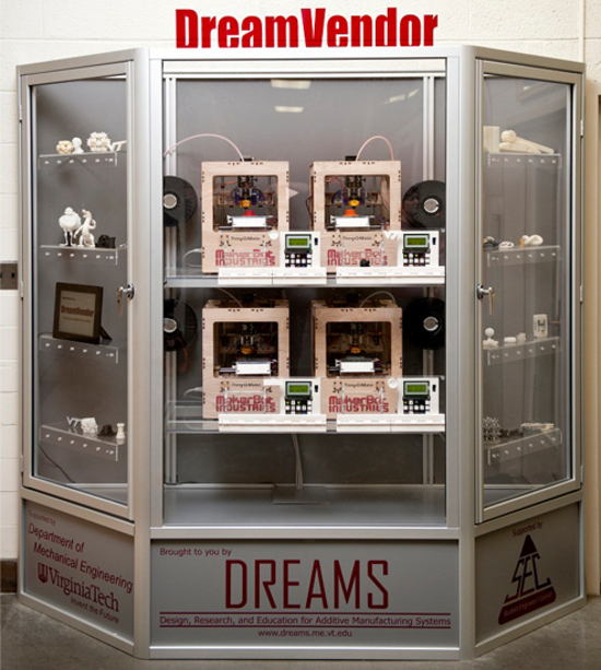
The popularity of 3D printing has exploded, but even as prices for the devices have fallen, not everyone is prepared or able to shell out the cash necessary start experimenting. But what if there was a 3D vending machine that made experimenting quick and easy, without the printer investment? Well, now there is.
Created at Virginia Tech's DREAMS Lab, the DreamVendor allows students to quickly print out prototype designs by simply inserting an SD card containing a physible data file into a large bank of four Makerbot Thing-O-Matic 3D printers. Once completed, the printed object is deposited into a vending-style retrieval shelf, similar to the one from which you might snag a candy bar or a bag of potato chips. Designed to encourage 3D prototyping at the lab, students are allowed to use the machine free of charge.
And while the school hasn't announced any plans to take the idea commercial, it's not difficult to imagine a day, in the very near future, when you'll see a similar, pay-per-3D-print version of the DreamVendor stationed at your local OfficeMax or Staples. You can see the DreamVendor in action in the video below.
Friday, November 16. 2012
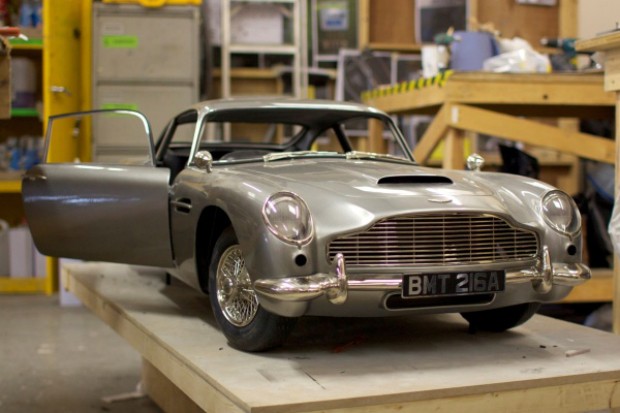
Misc. Gadgets Voxeljet 3D printer used to produce Skyfall's Aston Martin stunt double
Via engadget
-----
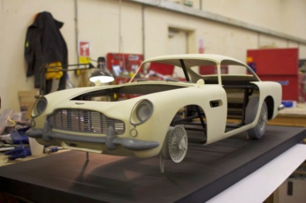
Spoiler alert: a reoccurring cast member bids farewell in the latest James Bond flick. When the production of Skyfall called for the complete decimation of a classic 1960s era Aston Martin DB5, filmmakers opted for something a little more lifelike than computer graphics. The movie studio contracted the services of Augsburg-based 3D printing company Voxeljet to make replicas of the vintage ride. Skipping over the residential-friendly MakerBot Replicator, the company used a beastly industrial VX4000 3D printer to craft three 1:3 scale models of the car with a plot to blow them to smithereens. The 18 piece miniatures were shipped off to Propshop Modelmakers in London to be assembled, painted, chromed and outfitted with fake bullet holes. The final product was used in the film during a high-octane action sequence, which resulted in the meticulously crafted prop receiving a Wile E. Coyote-like sendoff. Now, rest easy knowing that no real Aston Martins were harmed during the making of this film. Head past the break to get a look at a completed model prior to its untimely demise.
Tuesday, November 06. 2012
I.B.M. Reports Nanotube Chip Breakthrough
-----
SAN FRANCISCO — I.B.M. scientists are reporting progress in a chip-making technology that is likely to ensure that the basic digital switch at the heart of modern microchips will continue to shrink for more than a decade.
The advance, first described in the journal Nature Nanotechnology on Sunday, is based on carbon nanotubes — exotic molecules that have long held out promise as an alternative to silicon from which to create the tiny logic gates now used by the billions to create microprocessors and memory chips.
The I.B.M. scientists at the T.J. Watson Research Center in Yorktown Heights, N.Y., have been able to pattern an array of carbon nanotubes on the surface of a silicon wafer and use them to build hybrid chips with more than 10,000 working transistors.
Against all expectations, silicon-based chips have continued to improve in speed and capacity for the last five decades. In recent years, however, there has been growing uncertainty about whether the technology would continue to improve.
A failure to increase performance would inevitably stall a growing array of industries that have fed off the falling cost of computer chips.
Chip makers have routinely doubled the number of transistors that can be etched on the surface of silicon wafers by shrinking the size of the tiny switches that store and route the ones and zeros that are processed by digital computers.
The switches are rapidly approaching dimensions that can be measured in terms of the widths of just a few atoms.
The process known as Moore’s Law was named after Gordon Moore, a co-founder of Intel, who in 1965 noted that the industry was doubling the number of transistors it could build on a single chip at routine intervals of about two years.
To maintain that rate of progress, semiconductor engineers have had to consistently perfect a range of related manufacturing systems and materials that continue to perform at evermore Lilliputian scale.

I.B.M. Research Vials contain carbon nanotubes that have been suspended in liquid.
The I.B.M. advance is significant, scientists said, because the chip-making industry has not yet found a way forward beyond the next two or three generations of silicon.
“This is terrific. I’m really excited about this,” said Subhasish Mitra, an electrical engineering professor at Stanford who specializes in carbon nanotube materials.
The promise of the new materials is twofold, he said: carbon nanotubes will allow chip makers to build smaller transistors while also probably increasing the speed at which they can be turned on and off.
In recent years, while chip makers have continued to double the number of transistors on chips, their performance, measured as “clock speed,” has largely stalled.
This has required the computer industry to change its designs and begin building more so-called parallel computers. Today, even smartphone microprocessors come with as many as four processors, or “cores,” which are used to break up tasks so they can be processed simultaneously.
I.B.M. scientists say they believe that once they have perfected the use of carbon nanotubes — sometime after the end of this decade — it will be possible to sharply increase the speed of chips while continuing to sharply increase the number of transistors.
This year, I.B.M. researchers published a separate paper describing the speedup made possible by carbon nanotubes.
“These devices outperformed any other switches made from any other material,” said Supratik Guha, director of physical sciences at I.B.M.’s Yorktown Heights research center. “We had suspected this all along, and our device physicists had simulated this, and they showed that we would see a factor of five or more performance improvement over conventional silicon devices.”
Carbon nanotubes are one of three promising
technologies engineers hope will be perfected in time to keep the
industry on its Moore’s Law pace.
Graphene is another promising
material that is being explored, as well as a variant of the standard
silicon transistor known as a tunneling field-effect transistor.
Dr. Guha, however, said carbon nanotube materials had more promising performance characteristics and that I.B.M. physicists and chemists had perfected a range of “tricks” to ease the manufacturing process.
Carbon nanotubes are essentially single sheets of carbon rolled into tubes. In the Nature Nanotechnology paper, the I.B.M. researchers described how they were able to place ultrasmall rectangles of the material in regular arrays by placing them in a soapy mixture to make them soluble in water. They used a process they described as “chemical self-assembly” to create patterned arrays in which nanotubes stick in some areas of the surface while leaving other areas untouched.
Perfecting the process will require a more highly purified form of the carbon nanotube material, Dr. Guha said, explaining that less pure forms are metallic and are not good semiconductors.
Dr. Guha said that in the 1940s scientists at Bell Labs had discovered ways to purify germanium, a metal in the carbon group that is chemically similar to silicon, to make the first transistors. He said he was confident that I.B.M. scientists would be able to make 99.99 percent pure carbon nanotubes in the future.
Friday, November 02. 2012
U.S. looks to replace human surveillance with computers
Via c|net
-----
Security cameras that watch you, and predict what you'll do next, sound like science fiction. But a team from Carnegie Mellon University says their computerized surveillance software will be capable of "eventually predicting" what you're going to do.

Computerized surveillance can predict what people will do next -- it's called "activity forecasting" -- and eventually sound the alarm if the action is not permitted. Click for larger image.
(Credit: Carnegie Mellon University)Computer software programmed to detect and report illicit behavior could eventually replace the fallible humans who monitor surveillance cameras.
The U.S. government has funded the development of so-called automatic video surveillance technology by a pair of Carnegie Mellon University researchers who disclosed details about their work this week -- including that it has an ultimate goal of predicting what people will do in the future.
"The main applications are in video surveillance, both civil and military," Alessandro Oltramari, a postdoctoral researcher at Carnegie Mellon who has a Ph.D. from Italy's University of Trento, told CNET yesterday.
Oltramari and fellow researcher Christian Lebiere say automatic video surveillance can monitor camera feeds for suspicious activities like someone at an airport or bus station abandoning a bag for more than a few minutes. "In this specific case, the goal for our system would have been to detect the anomalous behavior," Oltramari says.
Think of it as a much, much smarter version of a red light camera: the unblinking eye of computer software that monitors dozens or even thousands of security camera feeds could catch illicit activities that human operators -- who are expensive and can be distracted or sleepy -- would miss. It could also, depending on how it's implemented, raise similar privacy and civil liberty concerns.

Alessandro Oltramari, left, and Christian Lebiere say their software will "automatize video-surveillance, both in military and civil applications."
(Credit: Carnegie Mellon University)A paper (PDF) the researchers presented this week at the Semantic Technology for Intelligence, Defense, and Security conference outside of Washington, D.C. -- today's sessions are reserved only for attendees with top secret clearances -- says their system aims "to approximate human visual intelligence in making effective and consistent detections."
Their Army-funded research, Oltramari and Lebiere claim, can go further than merely recognizing whether any illicit activities are currently taking place. It will, they say, be capable of "eventually predicting" what's going to happen next.
This approach relies heavily on advances by machine vision researchers, who have made remarkable strides in last few decades in recognizing stationary and moving objects and their properties. It's the same vein of work that led to Google's self-driving cars, face recognition software used on Facebook and Picasa, and consumer electronics like Microsoft's Kinect.
When it works well, machine vision can detect objects and people -- call them nouns -- that are on the other side of the camera's lens.
But to figure out what these nouns are doing, or are allowed to do, you need the computer science equivalent of verbs. And that's where Oltramari and Lebiere have built on the work of other Carnegie Mellon researchers to create what they call a "cognitive engine" that can understand the rules by which nouns and verbs are allowed to interact.
Their cognitive engine incorporates research, called activity forecasting, conducted by a team led by postdoctoral fellow Kris Kitani, which tries to understand what humans will do by calculating which physical trajectories are most likely. They say their software "models the effect of the physical environment on the choice of human actions."
Both projects are components of Carnegie Mellon's Mind's Eye architecture, a DARPA-created project that aims to develop smart cameras for machine-based visual intelligence.
Predicts Oltramari: "This work should support human operators and automatize video-surveillance, both in military and civil applications."
Thursday, November 01. 2012
Telefonica Digital shows off Thinking Things for connecting stuff to the web
Via Slash Gear
-----
Telefonica Digital has unveiled a new plastic brick device designed to connect just about anything you can think of to the Internet. These plastic bricks are called Thinking Things and are described as a simple solution for connecting almost anything wirelessly to the Internet. Thinking Things is under development right now.

Telefonica I+D invented the Thinking Things concept and believes that the product will significantly boost the development of M2M communications and help to establish an Internet of physical things. Thinking Things can connect all sorts of inanimate objects to the Internet, including thermostats and allows users to monitor various assets or tracking loads.
Thinking Things are comprised of three different elements. The first is a physical module that contains the core communications and logic hardware. The second element is energy to make electronics work via a battery or AC power. The third element is a variety of sensors and actuators to perform the tasks users want.
The Thinking Things device is modular, and the user can connect together multiple bricks to perform the task they need. This is an interesting project that can be used for anything from home automation offering simple control over a lamp to just about anything else you can think of. The item connected to the web using Thinking Things automatically gets its own webpage. That webpage provides online access allowing the user to control the function of the modules and devices attached to the modules. An API allows developers to access all functionality of the Thinking Things from within their software.
Quicksearch
Popular Entries
- The great Ars Android interface shootout (131533)
- Norton cyber crime study offers striking revenue loss statistics (102451)
- MeCam $49 flying camera concept follows you around, streams video to your phone (100547)
- The PC inside your phone: A guide to the system-on-a-chip (58719)
- Norton cyber crime study offers striking revenue loss statistics (58680)
Categories

Show tagged entries
Syndicate This Blog
Calendar
|
|
July '26 | |||||
| Mon | Tue | Wed | Thu | Fri | Sat | Sun |
| 1 | 2 | 3 | 4 | 5 | ||
| 6 | 7 | 8 | 9 | 10 | 11 | 12 |
| 13 | 14 | 15 | 16 | 17 | 18 | 19 |
| 20 | 21 | 22 | 23 | 24 | 25 | 26 |
| 27 | 28 | 29 | 30 | 31 | ||